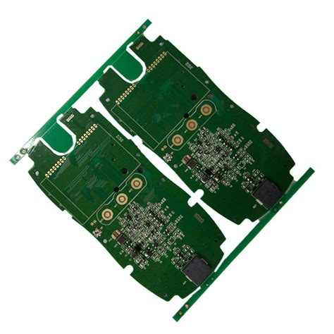
Using Allegro to implement high-speed circuit wiring design for embedded systems
1 Introduction
With the continuous increase in the main frequency of embedded microprocessors, the transmission and processing speed of signals is getting faster and faster.
When the system clock frequency reaches above 100MHZ, traditional circuit design methods and software can no longer meet the requirements of high-speed circuit design. In high-speed circuit design, the equal length of routing, impedance control of key signals, and setting of differential routing are becoming more and more important.
The author’s Wuhan Huazhong University of Science and Technology cooperated with the Intelligent Instrument Room of the Institute of Rock and Soil Mechanics of the Chinese Academy of Sciences in Wuhan.
The embedded system with ARM9 microprocessor EP9315 as the core completed the development of engineering detection instrument. Among them, the equal length routing of SDRAM and IDE, impedance control of key signals and differential routing in the hardware circuit design of the embedded system are the focus of this article. At the same time, the network physical layer interface 13 chip cs8952 of Cirrus Logic Company is used as an example to introduce the hardware circuit design of the network part in detail, providing a reference method for similar high-speed hardware circuit design.

2 Hardware Platform
2.1 Main Chips
The embedded microprocessor used in this design is the high-end product EP9315 in the EP93XX series launched by Cirrus Logic in July 2004. This microprocessor is a highly integrated system-on-chip processor with an ARM920T core operating at a frequency of 200 MHz.
It has all the excellent performance of the ARM920T core, including rich integrated peripheral interfaces including PCMCIA, interface graphics accelerator, EIDE that can connect two sets of devices, 1/10/100Mbps Ethernet MAC, 3 2.0 full-speed HOST USBs, LCD interface of dedicated SDRAM channel, touch screen interface, SPI serial peripheral interface, AC97 interface, 6-channel I2S interface and 8*8 keyboard scan interface. It also supports seamless connection of 4 groups of 32-bit SDRAM, etc.
The main chip’s rich peripheral interfaces greatly simplify the system hardware circuit. Except for the network control part that uses Cirrus Logic’s 100Base-X/10Base-T physical layer (PHY) interface chip CS8952, other functional modules do not need to add additional control chips.

2.2 System Main Structure
As shown in Figure 1, the system is based on the microprocessor EP9315, has complete peripheral interface functions, and controls the engineering detector at the same time. The IDE/CF card interface provides a large-capacity mobile storage device for engineering detection data; the 32M SDRAM is expanded as an external data storage space; 3 active USB interfaces support USB keyboard and mouse; the LCD interface supports STN/TFT liquid crystal and touch screen. Provides a friendly interactive interface for users; 1/10/100 Mbps Ethernet provides a way to download the kernel when debugging the operating system and remote monitoring during engineering detection; the panel buttons provide a human-computer interaction interface for engineers who cannot use keyboards and mice when working in the field.
EP9315 has a main frequency of 200M, a bus frequency of 100M, and a peripheral clock of 50M under the operating system.
The wiring density of data lines and address lines is large and the speed is high. The network part has special requirements for differential lines and microstrip line control. In the past, Protel design was mainly used for PCB layout and wiring based on experience. Obviously, this method cannot meet the current high-speed circuit design. As one of the largest companies in the EDA field, CADENCE’s PCB design tool performance advantages are becoming more and more obvious in high-speed circuit design. Therefore, the author uses CADENCE’s PCB design layout software Allegro to complete high-speed circuit design.

3 Design Implementation
3.1 SDRAM Wiring Rules
The embedded system uses a 64M-byte SDRAM extended data storage area, which consists of two K4S561632 chips working in 32-bit mode. The highest frequency can reach more than 100M. For the data line, clock line, chip select and other control signals of SDRAM, the line length needs to be matched, so the following wiring requirements are proposed:
- SDRAM clock signal: The clock signal frequency is relatively high. In order to avoid the transmission line effect, the wiring length should be within 1000mil when the operating frequency reaches or exceeds 75MHz, and to avoid crosstalk with adjacent signals. The routing length does not exceed 1000mil, the line width is 10mil, the internal spacing is 5mil, and the external spacing is 30mil. Differential routing is required, and the differential pair routing is accurately matched. The error is allowed to be within 20mil.
- Address, chip select and other control signals: line width is 5mil, external spacing is 12mil, and internal spacing is 10mil. Try to make a daisy chain topology. It can effectively control high-order harmonic interference and can be longer than the clock line, but not shorter.
- SDRAM data line: line width 5mil, internal spacing 5mil, external spacing 8mil, try to route on the same layer, and control the line length difference between data line and clock line within 50mil.
According to the routing requirements, set different constraints in Allegro: set 3 constraints SDRAM_CLK, SDRAM_ADDDR, SDRAM_DATA for line width, and add the constraints to the corresponding net after setting the constraints. Make each net have line width and line spacing constraint attributes. Finally, select the appropriate constraints for different signal groups. However, the set constraints cannot be achieved inside the system CPU. Because EP9315 is a BGA package. The pin spacing is 1.27 mm. Obviously, inside the CPU, the line width and line spacing cannot meet the above requirements. Use Allegro to set the CPU special routing area cpu_area. And add the area attribute, and set constraints suitable for BGA internal routing in this area.


