Very detailed BUCK circuit PCB layout suggestions
In the application design of DC-DC chips, whether the PCB layout is reasonable has a crucial impact on whether the chip can show its optimal performance. Unreasonable PCB layout will cause the chip performance to deteriorate, such as linearity reduction (including input linearity and output linearity), load capacity reduction, unstable operation, increased EMI radiation, increased output noise, etc., and more seriously, it may directly cause chip damage.
Generally, the user manual of DC-DC chips will have its corresponding PCB layout design requirements and layout schematics. This time, we will take the synchronous BUCK chip as an example to briefly talk about the PCB Layout design points in the application design of DC-DC chips.
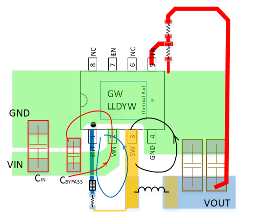
1.Pay attention to the high current path of the chip
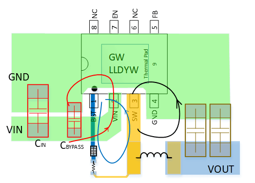
DC-DC chip layout must follow a very important principle, that is, the area of the switching high current loop should be as small as possible. In the BUCK topology shown in the figure below, it can be seen that there are two large current loops in the chip switching process. The red is the input loop and the green is the output loop. Each current loop can be regarded as a loop antenna, which will radiate energy to the outside and cause EMI problems. The size of the radiation is proportional to the loop area.
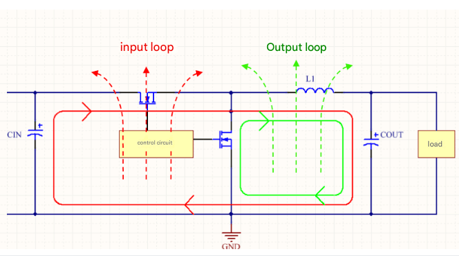
(Note: When the chip pin settings are not enough for us to take into account the minimum of both the input loop and the output loop, for BUCK, the input loop wiring optimization should be given priority. Because the current in the output loop is continuous, while the current in the input loop is jumping, it will produce a larger di/dt, which is more likely to cause EMI problems. If it is a BOOST chip, the output loop wiring optimization should be given priority.) Learn hardware, practice makes perfect, combine theory with practice, and do more summary!
2. Input capacitor configuration
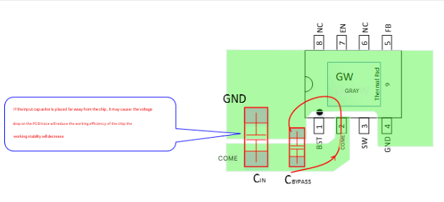
① For BUCK chips, in order to make the input loop as small as possible, the input capacitor should be placed as close to the chip pin as possible;
② In order to make the capacitor filtering effect better, let the power pass through the input capacitor first and then enter the chip;
③ The large-capacity capacitor used by CIN generally has poor frequency characteristics, so a high-frequency decoupling capacitor CBYPASS with good frequency characteristics should be connected in parallel with CIN;
④ In the case of a power supply with small current capacity (IO≤1A), the capacitance value also becomes smaller, so sometimes a ceramic capacitor can be used to have both CIN and CBYPASS functions;
3.Inductor configuration
① For BUCK chips, in order to make the input loop as small as possible, the inductor should be placed close to the chip SW pin;
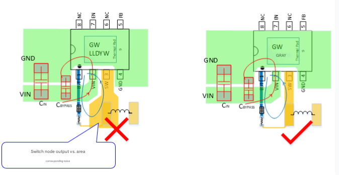
② Use copper-clad routing to reduce parasitic inductance and resistance;
③ The SW node should handle large currents with the smallest area to prevent the copper foil area from becoming larger and acting as an antenna, so that EMI increases;
④ Do not run sensitive signal lines near the inductor;
⑤ For the bootstrap circuit, the bootstrap circuit should be as close to the SW pin as possible to shorten the entire high-frequency flow path;
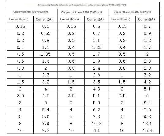
Attached is the corresponding relationship between the line width, copper thickness and current of the PCB board when the temperature rises by 10℃ for reference.
4.Output capacitor configuration
In the buck converter, the output current is smooth because the inductor is connected in series to the output;
The output capacitor is placed close to the inductor;
5.Feedback path wiring
① Usually the voltage divider resistor at the FB feedback network adopts K-level, 10K-level or hundreds of K resistance. The larger the resistance, the more susceptible to interference. It should be kept away from various noise sources such as inductors, SW, freewheeling diodes, etc.;
② The signal ground of the FB and COMP pins should be isolated from the power ground with large current as much as possible, and then connected at a single point. Try not to let the ground of large current signals interfere with the ground of small signal current;
③ The voltage divider resistor of FB needs to be sampled from VOUT, and the sampling point should be close to the output capacitor to obtain a more accurate actual output voltage value;