Vias in high speed pcb design
Vias are an essential component in high-speed PCB design.
They are used to connect different layers of the PCB and provide a path for electrical signals to pass through.
In high-speed PCB design, vias play a critical role in maintaining signal integrity and reducing electromagnetic interference (EMI).
There are several types of vias used in high-speed PCB design,
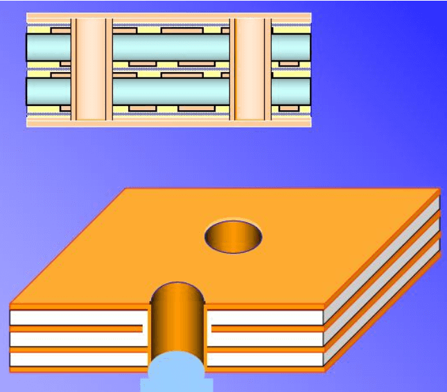
including through-hole vias, blind vias, and buried vias.
Through-hole vias are the most common type of via and are used to connect all layers of the PCB.
Blind vias are used to connect the outer layer of the PCB to the inner layer, while buried vias are used to connect the inner layers of the PCB.
To ensure optimal signal integrity and reduce EMI, it is important to carefully design and place vias in high-speed PCBs.
This includes using the appropriate via size, spacing, and placement, as well as ensuring proper impedance matching and signal routing.
It is also important to consider the manufacturing process and the cost of the PCB when designing vias.
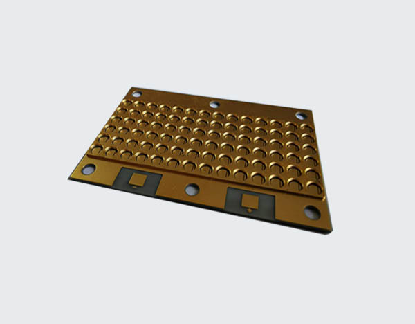
the role of vias in high speed pcb design
Vias play an important role in high-speed PCB design as they provide a means of connecting different layers of the PCB and routing signals between them.
In high-speed designs, signals travel at high frequencies and require a low impedance path to ensure signal integrity.
Vias can be used to create a low impedance path between different layers of the PCB, reducing the signal’s return path and minimizing the risk of electromagnetic interference (EMI).
Vias can also be used to reduce the length of signal traces, which can help to minimize signal delay and improve signal quality.
By placing vias directly under components, designers can reduce the length of the signal trace and minimize the parasitic capacitance and inductance that can degrade signal quality.
In addition, vias can be used to create a ground plane that can help to reduce EMI and improve signal quality.
By placing vias around the signal traces, designers can create a ground plane that provides a low impedance path for return currents, reducing the risk of EMI.
Overall, vias are an essential component of high-speed PCB design, providing a means of connecting different layers of the PCB,
reducing signal delay, minimizing EMI, and improving signal quality.
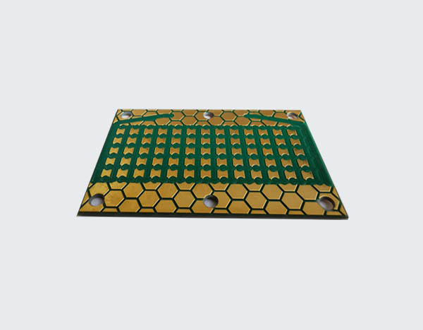
high speed pcb layer stack up
A high speed PCB layer stack up typically consists of multiple signal layers,
ground and power planes, and sometimes a dedicated layer for high speed signals.
The layer stack up is designed to minimize signal interference and crosstalk, and to provide a low impedance path for power and ground.
The number and arrangement of layers can vary depending on the specific design requirements, but typically include:
1. Signal layers:
These are the layers that carry the actual signals in the circuit.
They are typically arranged in pairs, with each pair consisting of a signal layer and a return plane layer.
The signal layers are usually placed adjacent to each other to minimize crosstalk and interference.
2. Ground plane:
This is a layer that is dedicated to providing a low impedance path for ground.
It is typically placed adjacent to the signal layers to provide shielding and reduce noise.
3. Power plane:
This is a layer that is dedicated to providing a low impedance path for power.
It is typically placed adjacent to the ground plane to reduce noise and provide a stable power supply.
4. High speed signal layer:
This is a dedicated layer for high speed signals, such as clock signals or high frequency data signals.
It is typically placed between the signal layers and the ground plane to provide shielding and reduce crosstalk.
The layer stack up is designed to balance the needs of signal integrity, power distribution, and thermal management.
It is an important aspect of high speed PCB design, and can have a significant impact on the performance of the circuit.

high speed pcb layout design
High speed PCB layout design is the process of designing printed circuit boards that can handle high frequency signals without distortion or loss of signal integrity. This type of design requires careful consideration of signal routing, component placement, and grounding techniques to minimize signal reflections, crosstalk, and noise.
Some key considerations for high speed PCB layout design include:
1. Signal routing:
High speed signals should be routed on the shortest possible path, with minimal bends and turns.
Differential pairs should be routed together and kept parallel to minimize crosstalk.
2. Component placement:
Components should be placed in a way that minimizes signal path length and reduces the risk of interference.
High speed components should be placed close to each other and near the edge of the board to minimize signal loss.
3. Grounding:
Proper grounding is critical for high speed PCBs. Ground planes should be placed on both sides of the board to provide a low impedance return path for signals.
Ground vias should be placed near high speed components to reduce noise and interference.
4. Power delivery:
High speed circuits require stable and clean power. Power planes should be placed on both sides of the board to provide a low impedance power delivery network.
Decoupling capacitors should be placed near high speed components to reduce noise and voltage fluctuations.
5. EMI/EMC considerations:
High speed PCBs are susceptible to electromagnetic interference (EMI) and electromagnetic compatibility (EMC) issues.
Shielding and filtering techniques should be employed to reduce EMI/EMC issues.
Overall, high speed PCB layout design requires careful planning and attention to detail to ensure optimal signal integrity and performance.

