Wave Soldering Process and Debugging Techniques
Introduction
Wave soldering is a widely used soldering technique in the electronics manufacturing industry, primarily for through-hole components (THT) and some surface-mount devices (SMD). This process involves passing a printed circuit board (PCB) over a molten solder wave to form reliable electrical connections. Due to its efficiency and consistency, wave soldering remains a critical process in high-volume production.
This article explores the wave soldering process, key parameters affecting soldering quality, and essential debugging techniques to optimize performance and minimize defects.
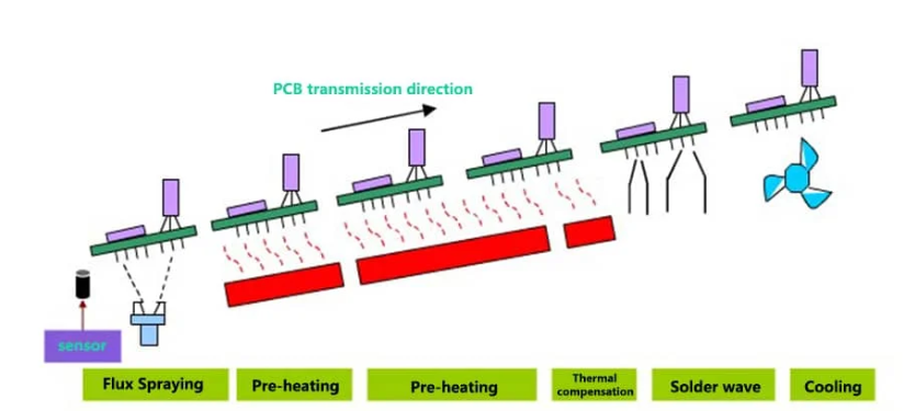
1. Wave Soldering Process Overview
The wave soldering process consists of several stages:
1.1 Flux Application
Before soldering, flux is applied to the PCB to remove oxides and improve solder wettability. Common flux application methods include:
- Spray Fluxing: Uses a nozzle to spray flux evenly.
- Foam Fluxing: A foam generator applies flux through a bubbler.
- Selective Fluxing: Targets specific areas to reduce waste.
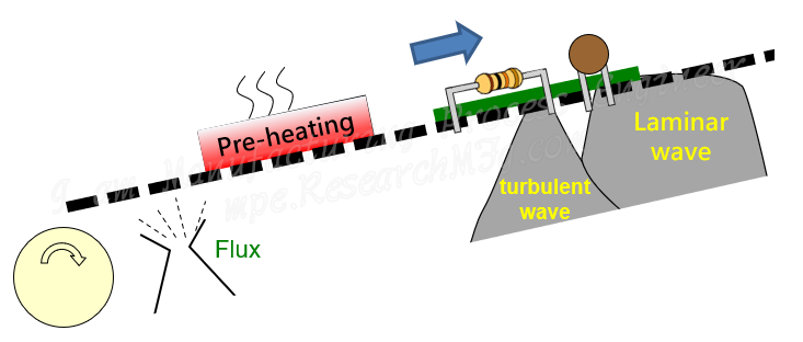
1.2 Preheating
The PCB is preheated to:
- Activate the flux.
- Reduce thermal shock during soldering.
- Evaporate solvents to prevent solder splashing.
Typical preheating temperatures range between 80°C–120°C.
1.3 Wave Soldering
The PCB passes over a molten solder wave (usually Sn-Pb or lead-free alloys like SAC305). The wave consists of two phases:
- Chip Wave (First Wave): A turbulent wave that ensures solder penetration.
- Laminar Wave (Second Wave): A smooth wave for proper fillet formation.
1.4 Cooling
After soldering, the PCB is cooled to solidify the joints and prevent thermal stress.
2. Key Parameters Affecting Wave Soldering Quality
Several factors influence soldering performance:
| Parameter | Optimal Range | Impact on Soldering |
|---|---|---|
| Solder Temperature | 250°C–265°C (Lead-free: 260°C–270°C) | Too low: Poor wetting; Too high: Oxidation & component damage |
| Contact Time | 2–5 seconds | Insufficient time: Cold joints; Excessive time: Thermal damage |
| Wave Height | 5–10 mm | Affects solder penetration and bridging risk |
| Flux Density | 0.80–0.85 g/cm³ | Low density: Poor wetting; High density: Residue buildup |
| Conveyor Speed | 0.8–1.8 m/min | Too fast: Incomplete soldering; Too slow: Overheating |
3. Common Wave Soldering Defects & Causes
| Defect | Possible Causes | Solutions |
|---|---|---|
| Bridging (Solder Shorts) | Excessive solder, incorrect wave height, poor PCB design | Adjust wave height, optimize pad spacing, check conveyor angle |
| Cold Joints | Low solder temperature, insufficient flux, fast conveyor speed | Increase temperature, ensure proper fluxing, reduce speed |
| Solder Balls | Flux splashing, excessive preheat, moisture on PCB | Adjust flux spray, control preheat, bake PCBs if necessary |
| Insufficient Fill | Low wave height, poor flux activity, incorrect contact time | Increase wave height, use active flux, extend dwell time |
| Voiding | Trapped gas, contaminated solder, poor hole wettability | Use nitrogen atmosphere, maintain solder purity, optimize flux |
4. Debugging Techniques for Optimal Wave Soldering
4.1 Optimizing Flux Application
- Adjust Spray Pressure: Too much flux causes splashing; too little leads to poor wetting.
- Check Nozzle Alignment: Ensure uniform coverage.
- Monitor Flux Density: Regularly measure and adjust as needed.
4.2 Controlling Solder Wave Dynamics
- Wave Height Adjustment: Should allow full penetration without excessive solder.
- Wave Shape Tuning: Balance between turbulent (penetration) and laminar (smoothing) waves.
- Nitrogen Blanketing: Reduces oxidation for lead-free solders.
4.3 Temperature Profiling
- Preheat Zone: Should gradually raise PCB temperature to avoid warping.
- Peak Solder Temperature: Must stay within alloy specifications.
- Cooling Rate: Should be controlled to prevent thermal stress cracks.
4.4 PCB Design Considerations
- Component Orientation: Avoid shadowing effects where solder cannot reach leads.
- Pad & Hole Size: Ensure proper solder flow and fillet formation.
- Thermal Relief Pads: Prevent heat sinking in large copper areas.
4.5 Maintenance & Process Monitoring
- Regular Solder Pot Analysis: Check for contamination (Cu, Fe) and dross removal.
- Nozzle & Machine Cleaning: Prevents flux buildup and wave instability.
- Automated Optical Inspection (AOI): Detects defects early for process adjustment.
5. Conclusion
Wave soldering remains a vital process in electronics manufacturing, but achieving consistent quality requires precise control of parameters such as temperature, flux application, wave dynamics, and conveyor settings. By understanding common defects and applying systematic debugging techniques, manufacturers can optimize yield and reliability.
Regular maintenance, real-time monitoring, and adherence to best practices ensure efficient wave soldering operations, reducing rework costs and improving product performance.


