What are Common PCB Manufacturing Defects?
Introduction
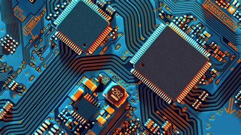
PCBs (printed circuit boards) are essential to most modern hardware. However, they are prone to defects during the manufacturing process. These defects can lead to disappointing PCBs and negatively impact product performance and consistent quality.
This comprehensive guide analyzes the most significant PCB manufacturing deserts, examines their underlying drivers, and provides potential answers to limited opportunities. PCBs consist of conductive copper traces stacked on an insulating substrate. Components are soldered to the board to form functional electronic circuits.
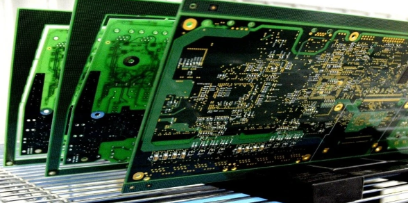
At every manufacturing stage, issues can arise that lead to defects in the finished circuit board. Common defects include soldering, mechanical damage, contamination, dimensional inaccuracies, plating defects, internal layer misalignment, drilling problems, and material issues.
PCB Defects and Quality Control: Addressing and minimizing these common PCB manufacturing defects is crucial as we strive to maintain high standards of quality and efficiency.
These defects can lead to electrical shorts, opens, poor aesthetics, reduced reliability, and even complete PCB failure.
Common PCB Manufacturing Defects
A deeper understanding of the primary causes of PCB defects enables manufacturers to implement robust process control and inspection methods to minimize risk. This article explores the most common PCB manufacturing defects, their root causes, and potential solutions.
Detecting and resolving defects early in the process is critical to reducing scrap and avoiding functional issues in the final product. Close collaboration with PCB manufacturers and communicating quality and defect prevention expectations will yield positive results. This guide covers strategies for minimizing defects through design, process control, inspection, training, and other methods.
Primary Causes of PCB Defects
Design defects and manufacturing variability are two of the primary causes of PCB defects. The following are a few of the main causes of common PCB manufacturing defects:
PCB manufacturing involves many complex steps, including design, imaging, etching, drilling, plating, solder mask application, screen printing, routing, and assembly. Multiple variables can lead to defects at each stage if not properly controlled. Understanding the key drivers of PCB defects allows for preventative measures.
Improper Design
Many PCB defects stem from design issues. Common design-related causes include insufficient spacing between traces, small annular rings around drilled holes, sharp trace angles that exceed manufacturing capabilities, and tolerances for fine lines or gaps that are impossible for the manufacturing process to achieve.
Other examples include symmetrical patterns that pose a risk of acid trapping, thin traces that can be damaged by electrostatic discharge, and thermal issues. Performing a comprehensive Design for Manufacturability (DFM) analysis and adhering to PCB design guidelines can prevent many design-induced defects.
Involving manufacturing engineers in the design process helps assess manufacturability. Simulation and modeling tools can also verify a design’s resistance to real-world stresses and identify problem areas. Optimizing design for manufacturability is a critical first step in minimizing common PCB manufacturing defects.
Contamination
PCB manufacturing involves the use of many chemicals and processes that can lead to contamination. During the manufacturing process, PCBs are susceptible to contamination from substances such as flux residue, finger oils, acidic plating solutions, particulate debris, and cleaning agent residues.
Contaminants pose the risk of electrical shorts, opens, solder defects, and long-term corrosion problems. Maintaining extremely clean production areas, implementing strict contamination controls, and preventing human contact minimizes the risk of contamination. Employee training on proper handling procedures is also crucial.
Material Defects
Materials used in PCB manufacturing must be free of inherent defects. Substandard PCB materials (such as low-quality laminates, prepregs, foils, and other components) may contain defects such as insufficient resin, protruding glass fibers, pinholes, and nodules.
These material defects can be incorporated into the final board and affect performance. Ensuring that all materials are sourced from reputable suppliers with extensive quality controls can help avoid material-related issues. Incoming material inspection is also recommended.
Mechanical Damage
Mechanical Damage to PCBs
PCBs are thin, fragile components susceptible to mechanical damage during the manufacturing process. Impacts, scratches, bending, dents, and other sources can cause physical damage. PCBs come into contact with numerous surfaces, fixtures, and handling equipment throughout the production process.
Well-designed handling procedures and fixtures are designed to minimize contact points, helping to prevent mechanical damage. It is also important to train employees in the correct techniques for loading, moving, and storing PCBs. Inspecting boards between process steps can detect damage early.
Process Variation
Normal process variation can cause PCB defects if critical parameters fall outside of control. Common examples include inaccurate etchant temperature, off-target drill speeds, misaligned lamination, and poor storage conditions.
Using statistical methods to monitor the process can detect deviations from required tolerances. Control charts provide a visual tool for maintaining the manufacturing process in a state of statistical control, thereby minimizing defects related to variability.
Human Error
Despite best efforts to prevent these errors, human errors are inevitable in PCB production. Machine operators may misload boards into plating tanks, use incorrect drill bit sizes, improperly store finished boards, and make other mistakes that can damage PCBs or create defects.
Comprehensive training programs, detailed work instructions, work aids such as checklists, and increased automation all help reduce human error. Redundancy through programs like secondary verification of machine settings can also accommodate errors before they impact the final product.
Common PCB Manufacturing Defects
Let’s now explore some of the most common PCB manufacturing defects:
A variety of potential PCB defects can occur during the manufacturing process. Awareness of the most prevalent manufacturing issues allows factories to appropriately focus inspection and process control efforts. The following are some of the most common PCB defects.
Soldering Defects
PCB Soldering Defects
Most PCB defects originate from the assembly process of soldering components to the board. Common soldering defects include:
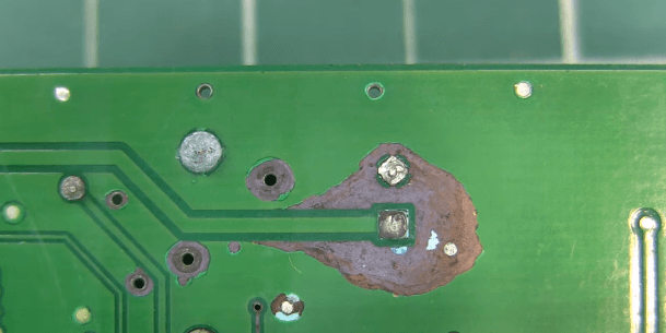
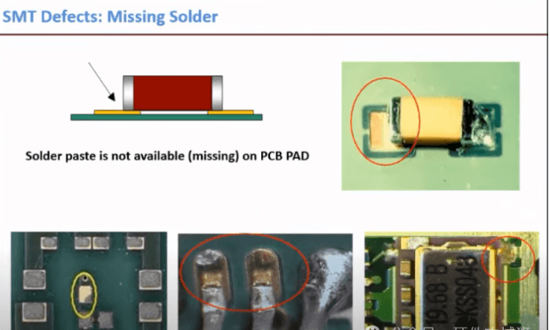
Soldering is a critical PCB assembly process that, if performed improperly, is prone to a variety of defects. Implementing strict protocols and inspection techniques can minimize soldering-related defects. Common soldering issues include bridging, voids, cold joints, solder balls, tombstoning, and insufficient wetting.
Solder bridges occur when solder inadvertently connects two areas that should remain electrically isolated. Excessive solder and component misalignment during reflow are common causes.
Solder voids occur when solder is missing from a joint. They reduce mechanical strength and conductivity. They are caused by surface contamination, poor wetting, poor solder quality, and low heat.
Cold solder joints occur when solder joints are incompletely wetted between surfaces due to insufficient heat during the soldering process. This increases resistance.
Solder balls occur when small balls of solder form independent masses. They can cause short circuits. They are often caused by spatter during hot air reflow.
Solder starvation occurs when insufficient solder is applied, resulting in fillets around joints. This can lead to poor connections and reliability issues.
Tombstone phenomenon occurs when one end of a surface mount component lifts off the board during reflow due to thermal imbalance during the soldering process.
Mechanical damage
Mechanical damage is one of the most common defect categories. PCBs can be damaged by the following reasons:
The thin and fragile nature of PCBs makes them susceptible to mechanical damage during the manufacturing process due to impact, scratches, bending, and other causes. Maintaining proper handling procedures and fixtures can minimize the risk. Common mechanical defects include:
Dents—localized depressions in the PCB surface that can crack the copper and reduce trace spacing. Scratches—areas where the cover material is rubbed away, exposing the base material. These can affect spacing and cause shorts or opens. These are often caused by contact with fixtures.
Warp—a distortion of the overall flatness of the PCB. This affects soldering processes and assembly. It is caused by bending the board due to thermal stress or improper handling.
Cracks—cracks in the PCB base and copper that can damage electrical connections. They form when bending stress exceeds the material’s limits.
Voids—complete punctures through the board, destroying the circuitry. These are often caused by contact with sharp objects during handling.
Chips—small fragments break off the edge of the PCB, resulting from collisions between boards during storage and handling.
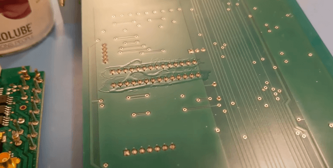
Contamination
PCB manufacturing presents multiple opportunities for contamination:
Many contaminants are unintentionally introduced during the PCB manufacturing process. These include flux residue, finger oils, metal particles, chemical solutions, dust, and other debris. Contamination can cause short circuits, damaged solder joints, leakage current, and corrosion.
Flux residue – Rosin-based flux remaining after soldering components. Over time, this can cause leakage current.
Finger oils – Skin oils deposited on the PCB surface due to handling. This interferes with soldering and can cause electrochemical migration.
Metal particles – Tiny metal fragments deposited on the PCB. This can cause short circuits and hinder soldering.
Chemical solutions – Plating solutions, solvents, and etchants leave residues after drying on the board. This promotes corrosion.
Dust/debris – Particles collected during the production process. This can impair soldering, assembly, and operational reliability.
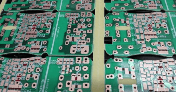
Dimensional Defects
PCBs must meet tight dimensional tolerances. Common Accuracy Issues:
Maintaining tight dimensional tolerances is critical to achieving proper PCB functionality. Common dimensional defects include:
Tilt – Misalignment between layers causes inner layers to shift. This can create shorts or opens.
Pattern misregistration – Layers are not properly aligned, resulting in misalignment of features such as holes.
Hole misalignment – Drilled holes are not located correctly as expected, hindering proper assembly.
Hole misalignment
Annular ring – The annular ring around the drilled hole is incorrectly sized according to specifications, affecting hole wall adhesion.
Out-of-tolerance features – Traces, spaces, holes, and other features that exceed the specified tolerances can cause shorts or reliability issues.
Board warpage – Overall, the warpage of the PCB exceeds the allowable flatness tolerance. This makes assembly difficult.
Plating defects
High-quality PCB plating is critical. Typical Plating Defects:
The plating on a PCB must be consistent and defect-free to achieve proper electrical connections and soldering. Common plating defects include:
Nodules—isolated bumps on the copper plating surface. In severe cases, these bumps can bridge gaps and cause shorts.
Pits—small voids and depressions in the plating. These can lead to poor solder wetting and unreliable joints.
Poor Adhesion—The plating must adhere properly to the board surface. This can lead to peeling and reliability issues in the long term.
Dull Plating—A dull, matte finish with a rough, dull texture, rather than a smooth sheen, indicates substandard plating quality.
Thin Plating—The plating is thinner than the specification requires. It can wear more quickly under electrical loads.
Drilling Defects
Proper PCB drilling is crucial. Drilling defects include:
The drilled holes must be of excellent quality to achieve proper connections between layers. Common drilling defects include:
Breakage—Protruding glass fibers break around the drilled hole. This can affect the connection.
Smudge – Resin residue around holes after drilling. It can hinder plating adhesion.
Misshapen holes – Holes with imperfect roundness or diameter. This can lead to poor connections.
Burrs – Rough holes that reduce plating quality.
Hole placement – Holes that are incorrectly centered. This can hinder proper assembly and connection.
Via stubs – Blind and buried vias that only partially penetrate the dielectric layer.
Solutions to Prevent Common PCB Manufacturing Defects
There are many ways to reduce the risk of PCB defects:
While PCB defects can never be eliminated, there are several strategies to minimize their occurrence:
Design for Manufacturability (DFM) Analysis
Performing DFM analysis during the design phase can identify features that may be difficult to manufacture reliably. Designers can modify the layout to eliminate these manufacturability risks before board fabrication begins.
Involving engineers from the PCB manufacturer in the design process ensures that manufacturing knowledge is incorporated into the design. Simulation and modeling tools also verify that the design can withstand real-world stresses and meet specifications.
Process Control
Implementing robust process control is crucial for minimizing PCB defects caused by manufacturing variability. Statistical process control (SPC) techniques continuously monitor key process parameters to detect when they deviate from established control limits. Control charts provide a visual tool for maintaining statistical stability in the manufacturing process.
Some key processes that require control include:
Etching – Monitoring etchant temperature, conveyor speed, and solution chemistry ensures optimal etch quality. Detecting when these excursions fall outside acceptable ranges minimizes under/overetching.
Lamination – Controlling parameters such as applied pressure, temperature gradients, and alignment stop layer misregistration and skew defects.
Drilling – In-process measurements of drill wear, hole size, hole location, surface finish, and missed holes reduce drilling issues.
Electroplating – Tracking plating thickness, adhesion testing, surface roughness, and solution chemistry enables early detection of plating issues.
Soldermask – Controlling coating thickness, cure time, viscosity, and adhesion prevents soldermask defects.
Soldering – Monitoring profiles, peak temperature consistency, and wetting quality ensures strong, defect-free solder joints.
Critical inputs that impact quality must be identified and monitored at each process step. Statistical process control provides the tools to measure these inputs on each board and visualize when they exceed defined control limits.
Operator Training
Extensive training for machine operators is crucial to reducing human error that leads to PCB defects. Workers should have the information and skills to perform their manufacturing jobs properly and without defects. Training should cover:
Equipment Operation – Proper machine loading/unloading, startup/shutdown, calibration, preventative maintenance, and parameter adjustment procedures. Hands-on demonstrations ensure proficiency.
Handling Techniques – Delicate PCB handling methods to avoid scratches, drops, edge impacts, bending, and other sources of damage. Use protective racks, gloves, and cleanroom protocols.
Visual Standards – Detecting subtle PCB defects requires recognition skills. InspectionInspectors need standards to indicate defect types such as plating nodules, solder voids, and contamination.
Defect Identification – In addition to visual skills, training in electrical testing and inspection methods is provided to reliably identify PCB defects. Diagnostic skills are also required to pinpoint root causes.
Contamination Control – Contamination risks and methods to prevent finger oils, chemical residues, particles, fibers, and other substances from contacting PCBs during handling.
ESD Control – ESD hazards, proper use of wrist straps, grounded shoes, grounded equipment, and safe PCB handling to prevent electrostatic discharge damage.
A formal certification program verifies operator qualifications through testing. This ensures that each employee meets knowledge requirements before working independently. Regular recertification and refresher courses strengthen skills.
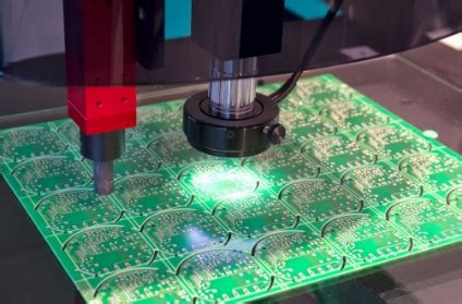
Inspection
Thorough inspection of PCBs at multiple manufacturing stages is crucial to detecting defects early, before they escalate. Both automated inspection systems and manual visual inspection should be used. Standard inspection methods include:
Automated Optical Inspection (AOI) – This uses cameras to image PCBs and employs sophisticated algorithms to identify defects that are undetectable to the human eye. Check for solder bridging, insufficient wetting, lifted leads, and contamination.
X-ray Inspection – X-ray imaging can identify defects such as voids in solder joints, clogged vias, and component mispositioning. It is particularly useful for discovering hidden defects.
Flying Probe Testing – Uses probes to inspect PCBs for electrical shorts and opens. It detects disconnects and damage not visible from the outside.
To ensure cleanliness, ionic cleanliness testing – Measures ionic residues from flux, finger oils, and other contaminants on the PCB surface.
Solder Paste Inspection – Inspects solder paste deposits for proper volume, offset, collapse, and bridging.
Visual Inspection – Manual visual inspection under a magnifying glass by trained quality technicians detects surface defects.
Frequent inspections at each major manufacturing step (imaging, etching, AOI, ICT, FPT, etc.) detect defects early. This allows defective boards to be reworked or scrapped, rather than further propagating the problem.
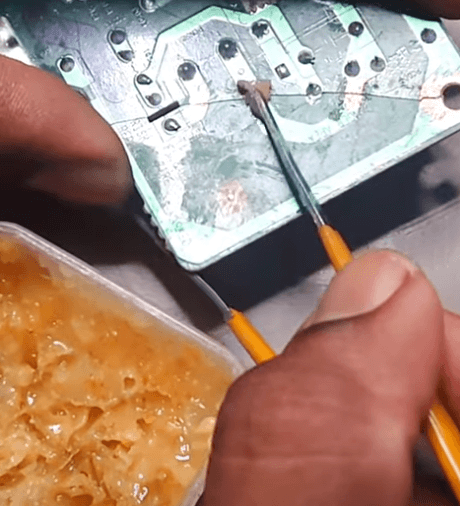
Contamination Control
Implementing strict contamination control is crucial to preventing particulate, chemical, and ESD-related PCB defects. Methods include:
Cleaning – Thorough cleaning between all wet process steps prevents chemical and debris accumulation on the circuit boards. Ultrasonic cleaning combined with a deionized water rinse effectively removes residues.
ESD Protocol – Wrist straps, ESD safety shoes, antistatic flooring, grounded work surfaces, ionizers, and humidity control prevent electrostatic discharge damage during handling.
Covering – Covering boards with lids or foam sheets when not actively processed prevents environmental particles from settling on the surface.
Gloves – Lint-free gloves must be used for all PCB handling to prevent oil and particulate matter from being transferred to bare hands when touching the circuit boards. Frequent glove changes maintain cleanliness.
Laminar Flow Hood – Assembly and inspection in a laminar flow hood use filtered airflow to prevent contaminants from contacting the PCBs.
Cleanroom – The ultimate contamination control environment. HEPA filters remove airborne particles, while sticky mats trap shoes. Personnel dress code procedures maintain cleanliness.
Training – Educating employees about contamination risks, cleaning methods, proper handling techniques, and contamination prevention is crucial.
Inspection – Ionic cleanliness testing frequently verifies that PCBs meet cleanliness specifications and identifies when process improvements are needed.
A clean, controlled environment is essential to eliminating contamination-related defects. Thorough onboard handling procedures and training maintain PCB cleanliness. Contamination control must be considered an integrated system encompassing materials, machines, employees, and facilities.
Traceability
Maintaining detailed records through Voyager or MES software allows PCBs to be traced back through the production process and materials to pinpoint the root cause when defects occur.
Traceability provides the data necessary for failure analysis. Records of machine parameters, test results, images, and material batches aid in troubleshooting.
Redundancy and Error-Proofing
Building in redundancy can accommodate inevitable human errors, such as secondary verification of machine settings and comparing Gerber files.
Error-Proofing through checklists, confirmation prompts, and process standardization reduces operator errors that impact quality.
Conclusion
Defects in PCB manufacturing occur due to design and manufacturing factors. Understanding the most common PCB defects allows factories to focus on targeted prevention and inspection efforts. Basic prevention principles include design analysis, strict process control, operator training, thorough inspection, cleanliness, board tracking, and error-proofing.