What Are Microwave Printed Circuit Boards and RF PCBs?
Introduction
In the rapidly advancing world of electronics, specialized circuit boards have become essential components for high-frequency applications. Microwave Printed Circuit Boards (PCBs) and Radio Frequency (RF) PCBs represent two critical categories of circuit boards designed to operate at high frequencies with minimal signal loss. These specialized boards enable modern wireless communication systems, radar technology, satellite communications, and numerous other high-frequency applications that form the backbone of our connected world.
While standard PCBs work well for low-frequency digital and analog circuits, they become increasingly inefficient as signal frequencies rise into the microwave and RF ranges. This article explores the fundamental concepts, design considerations, materials, manufacturing processes, and applications of Microwave PCBs and RF PCBs, highlighting their similarities, differences, and importance in modern electronics.
Understanding the Basics
Definition of Microwave PCBs
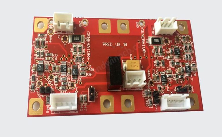
Microwave Printed Circuit Boards are specialized circuit boards designed to operate at frequencies typically ranging from 1 GHz to 100 GHz, covering the microwave portion of the electromagnetic spectrum. These boards are engineered to maintain signal integrity, minimize losses, and prevent unwanted radiation at these high frequencies where conventional PCB designs would fail.
Microwave PCBs are characterized by their precise dimensional control, specialized substrate materials, and careful attention to impedance matching. They often incorporate transmission line structures like microstrip or stripline rather than conventional traces to properly guide high-frequency signals.
Definition of RF PCBs
RF PCBs (Radio Frequency Printed Circuit Boards) are designed to handle frequencies generally ranging from a few MHz up to several GHz, covering the radio frequency spectrum. While there’s some overlap with microwave frequencies (typically considered above 1 GHz), RF PCBs focus on the challenges of maintaining signal integrity across the broader RF range.
The distinction between RF and microwave PCBs isn’t always clear-cut, as many design principles overlap. Generally, as frequencies increase into the microwave range, the design challenges become more stringent, requiring more specialized materials and fabrication techniques.
Key Differences Between RF and Microwave PCBs
While RF and microwave PCBs share many similarities, several key differences exist:
- Frequency Range: RF PCBs typically cover from 3 MHz to several GHz, while microwave PCBs focus on 1 GHz and above.
- Material Requirements: Microwave PCBs often require more advanced dielectric materials with tighter tolerances.
- Design Complexity: Microwave designs generally demand more precise control over impedance and propagation characteristics.
- Physical Dimensions: At microwave frequencies, even small board features can significantly affect performance, requiring more exacting manufacturing standards.
Design Considerations for High-Frequency PCBs
Impedance Control
Maintaining consistent characteristic impedance throughout the circuit is paramount in both RF and microwave PCB design. Common impedance values include 50Ω for most RF systems and 75Ω for video applications. Achieving proper impedance requires precise control over:
- Trace width and thickness
- Dielectric material thickness
- Dielectric constant of the substrate material
Signal Integrity
High-frequency designs must minimize several types of signal degradation:
- Insertion Loss: Reduction in signal power as it travels through the PCB
- Return Loss: Signal reflections due to impedance mismatches
- Crosstalk: Unwanted coupling between adjacent traces
- Radiation Losses: Energy lost to electromagnetic radiation
Transmission Line Structures
Instead of conventional traces, RF and microwave PCBs use specialized transmission line structures:
- Microstrip: A trace on the outer layer with a ground plane beneath
- Stripline: A trace embedded between two ground planes
- Coplanar Waveguide: A trace with adjacent ground planes on the same layer
- Slotline and Finline: More specialized structures for specific applications
Each type has advantages regarding shielding, loss characteristics, and fabrication complexity.
Material Selection
The choice of substrate material critically impacts the performance of RF and microwave PCBs. Key material properties include:
Dielectric Constant (Dk or εr)
The dielectric constant affects signal propagation speed and impedance. Materials with stable Dk across frequency and temperature are preferred. Common values range from 2.2 to 10.
Dissipation Factor (Df or tan δ)
This measures dielectric loss, with lower values being better for high-frequency applications. Microwave-grade materials typically have Df values below 0.005.
Thermal Properties
High-frequency circuits often generate significant heat, requiring materials with good thermal conductivity and stability.
Common PCB Materials
- FR-4: Standard material, limited to lower RF frequencies due to higher losses
- Rogers RO4000 Series: High-frequency laminates with excellent performance
- PTFE-Based Materials: (e.g., Rogers RT/duroid, Taconic TLY): Low-loss materials for demanding applications
- Ceramic-Filled PTFE: Offers good thermal and electrical properties
- Hydrocarbon Ceramics: Cost-effective alternative to PTFE for some applications
Manufacturing Challenges and Solutions
Precision Fabrication
Microwave and RF PCBs require exceptional manufacturing precision:
- Tight tolerances on trace widths (±0.025 mm or better)
- Controlled dielectric thickness
- Precise via formation
- Smooth copper surfaces to minimize skin effect losses
Plating and Surface Finishes
Surface finishes must maintain good conductivity while preventing oxidation:
- Electroless Nickel Immersion Gold (ENIG)
- Immersion Silver
- Electrolytic Hard Gold
- Organic Solderability Preservatives (OSP)
Via Technologies
Various via types address different needs:
- Through-Hole Vias: Standard vias spanning the entire board
- Blind Vias: Connect outer layers to inner layers without going through the entire board
- Buried Vias: Connect inner layers without reaching outer layers
- Microvias: Small vias (typically <0.15 mm) for high-density interconnects
Assembly Considerations
Component placement and soldering require special attention:
- Minimizing lead lengths for discrete components
- Proper grounding techniques
- Careful thermal management during soldering
- Use of chip-and-wire techniques for some microwave assemblies
Applications of RF and Microwave PCBs
Wireless Communication Systems
- Cellular base stations and mobile devices
- WiFi routers and access points
- Bluetooth devices
- 5G infrastructure
Aerospace and Defense
- Radar systems
- Electronic warfare systems
- Satellite communications
- Avionics
Automotive
- Collision avoidance radar
- Vehicle-to-vehicle communication
- GPS systems
- Keyless entry systems
Medical Equipment
- MRI systems
- RF ablation devices
- Medical imaging systems
- Wireless patient monitoring
Industrial and Scientific
- RF identification (RFID) systems
- Industrial heating equipment
- Scientific instrumentation
- Particle accelerators
Testing and Validation
Network Analysis
Vector Network Analyzers (VNAs) measure S-parameters to evaluate:
- Insertion loss
- Return loss
- Isolation between ports
- Phase characteristics
Time Domain Reflectometry (TDR)
TDR helps identify impedance discontinuities and locate faults in transmission lines.
Power Handling Tests
Verify that the PCB can handle required power levels without:
- Excessive heating
- Arcing or breakdown
- Performance degradation
Environmental Testing
Assess performance under various conditions:
- Temperature extremes
- Humidity
- Vibration
- Thermal cycling
Future Trends
Higher Frequency Applications
Emerging applications in:
- Millimeter-wave systems (30-300 GHz)
- THz technologies
- Advanced 5G and 6G systems
Advanced Materials
Development of new substrate materials with:
- Lower loss tangents
- More stable dielectric constants
- Better thermal properties
- Improved cost-effectiveness
Integration Technologies
- Embedded active and passive components
- 3D packaging approaches
- Heterogeneous integration
- Advanced interconnect technologies
Design Automation
Improved EDA tools for:
- Electromagnetic simulation
- Thermal analysis
- Automated optimization
- Manufacturing design rule integration
Conclusion
Microwave Printed Circuit Boards and RF PCBs represent specialized branches of PCB technology that enable modern high-frequency electronics. While sharing many common principles, microwave PCBs typically address more stringent requirements at higher frequencies. The design and manufacture of these boards involve careful consideration of materials, transmission line structures, impedance control, and signal integrity to ensure proper operation at their target frequencies.
As wireless technologies continue to advance into higher frequency ranges and support greater bandwidths, the importance of RF and microwave PCB technology will only grow. From 5G networks to advanced radar systems and beyond, these specialized circuit boards form the physical foundation that makes high-frequency electronics possible. Understanding their characteristics, requirements, and applications is essential for engineers working in wireless communications, defense, aerospace, and numerous other fields that rely on high-frequency signal processing.
The ongoing development of new materials, manufacturing techniques, and design tools promises to further enhance the capabilities of RF and microwave PCBs, enabling the next generation of high-frequency electronic systems that will continue to transform our technological landscape.