What are the causes of PCB failure?
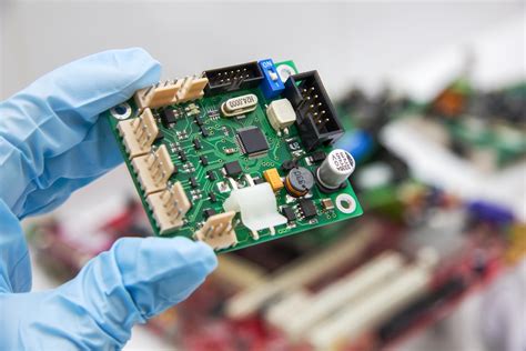
As the carrier of various components and the hub of circuit signal transmission, PCB has become an important and critical part of electronic information products. Its quality and reliability level determine the quality and reliability of the whole equipment.
With the miniaturization of electronic information products and the environmental protection requirements of lead-free and halogen-free, PCB is also developing in the direction of high density, high Tg and environmental protection. However, due to cost and technical reasons, a large number of failure problems have occurred in the production and application of PCB, which has caused many quality disputes. In order to find out the cause of failure in order to find a solution to the problem and clarify the responsibility, failure analysis must be performed on the failure that has occurred.
Basic procedures for failure analysis
To obtain the accurate cause or mechanism of PCB failure or defect, the basic principles and analysis process must be followed, otherwise valuable failure information may be missed, resulting in the inability to continue the analysis or possible wrong conclusions. The general basic process is that first, based on the failure phenomenon, the failure location and failure mode must be determined through information collection, functional testing, electrical performance testing and simple appearance inspection, that is, failure location or fault location.
For simple PCB or PCBA, the failure site is easy to determine. However, for more complex BGA or MCM packaged devices or substrates, defects are not easy to observe through a microscope and are not easy to determine at the moment. At this time, other means are needed to determine.
Then the failure mechanism analysis is carried out, that is, various physical and chemical means are used to analyze the mechanism that causes PCB failure or defects, such as cold solder joints, pollution, mechanical damage, moisture stress, dielectric corrosion, fatigue damage, CAF or ion migration, stress overload, etc.
Then there is the failure cause analysis, that is, based on the failure mechanism and process analysis, find the cause of the failure mechanism, and conduct experimental verification when necessary. Generally, experimental verification should be carried out as much as possible. Through experimental verification, the accurate cause of induced failure can be found.
This provides a targeted basis for the next step of improvement. That is, according to the test data, facts and conclusions obtained in the analysis process, the failure analysis is compiled, and the facts are clear, the logical reasoning is strict, and the logic is strong. Do not imagine out of thin air.
In the process of analysis, pay attention to the basic principle that the analysis method should be used from simple to complex, from outside to inside, and from not destroying the sample to using destruction. Only in this way can we avoid losing key information and introducing new artificial failure mechanisms.
Just like a traffic accident, if one party destroys or flees the scene, even the most skilled police can hardly make an accurate determination of responsibility. At this time, traffic regulations generally require the party who flees the scene or destroys the scene to bear all responsibilities.
The same is true for the failure analysis of PCB or PCBA. If a soldering iron is used to repair the failed solder joints or a large scissors is used to forcefully cut the PCB, then further analysis will be impossible because the failure site has been destroyed. Especially when there are few failed samples, once the environment of the failure site is destroyed or damaged, the real cause of failure cannot be obtained.
Failure analysis technology
Optical microscope
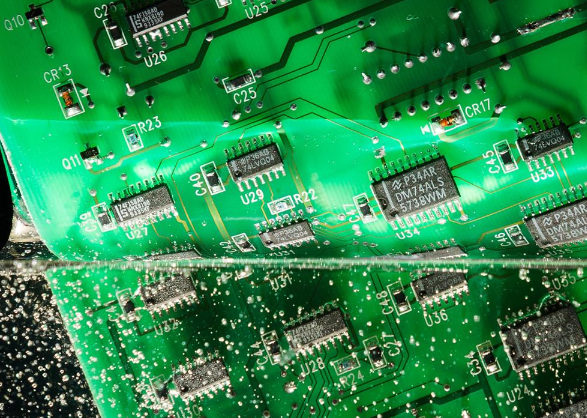
Optical microscope is mainly used for the appearance inspection of PCB, to find the failed parts and related physical evidence, and to preliminarily judge the failure mode of PCB. The appearance inspection mainly checks the pollution, corrosion, location of the burst board, circuit wiring, and the regularity of the failure, such as batch or individual, whether it is always concentrated in a certain area, etc.
X-ray
For some parts that cannot be inspected by appearance, as well as the internal defects of PCB through holes and other internal defects, we have to use X-ray fluoroscopy system to inspect.
X-ray fluoroscopy system uses different principles of moisture absorption or transmittance of X-rays by different material thickness or different material density to form images. This technology is more used to check defects inside PCBA solder joints, internal defects of through holes, and the location of defective solder joints of high-density packaged BGA or CSP devices.
Slice analysis
Slice analysis is the process of obtaining the cross-sectional structure of PCB through a series of means and steps such as sampling, inlaying, slicing, polishing, corrosion, and observation. Through slice analysis, rich information on the microstructure of PCB (through holes, plating, etc.) quality can be obtained, providing a good basis for the next step of quality improvement. However, this method is destructive. Once sliced, the sample will inevitably be destroyed.