What are the common specifications and precision requirements for PCB locating holes?
Today,a one-stop PCBA intelligent manufacturing company will explain what PCB locating holes are ,how to locate them ,and common specifications and precision requirements.To facilitate circuit board assembly and processing,locating holes are designed on PCBs.
What are PCB locating holes?
Circuit board locating holes are crucial for determining the specific location of PCB vias during the PCB design process.Locating holes serve as a processing reference during printed circuit board fabrication.There are various methods for locating PCB locating hole,primarily based on different positioning accuracy requirement.Locating holes on printed circuit board can be used as a substitute.
To facilitate board fixation during drilling and milling, as well as in-circuit testing, many PCB manufacturers require users to design three non-plated holes (PTHs) on the PCB. These holes are typically non-plated holes with a drill diameter of 6mm or 6.8mm. If board space is limited, at least two holes should be placed diagonally. For paneling, the panels can be considered a single PCB; the entire panel only needs three holes. If the user does not place these holes, the PCB manufacturer will automatically add them without affecting the circuitry, or use existing PTHs on the board as locating holes.
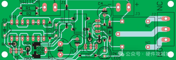
PTH Hole Positioning Methods
Device Holes: Interface components and connectors are mostly plug-in components. The diameter of the through-holes for plug-in components is 8 to 20 mils larger than the pin diameter, ensuring good solder penetration during soldering. It’s important to note that the hole diameters specified by the PCB manufacturer vary, generally within ±0.05mm. Drills are assigned a different drill bit every 0.05mm. For diameters larger than 3.20mm, drills are assigned a different drill bit every 0.1mm. Therefore, when designing component apertures, convert the units to millimeters and design the apertures to integer multiples of 0.05. The PCB manufacturer sets the drill tool size based on the user-provided drilling data. The drill tool size is typically 0.1 to 0.15 mm larger than the user’s desired finished hole. The designed aperture diameter should be larger rather than smaller, and the tolerance should also be larger rather than smaller. The fewer aperture types, the better. For press-fit components, do not enlarge the aperture diameter; design according to the documentation recommendations. The PCB design instructions should specify which components are press-fit. This allows the PCB manufacturer to minimize errors during the PCB design process and avoid unnecessary trouble.
PCB Design Positioning Hole Requirements and Specifications
Drilled holes are categorized as plated-through holes (PTH) and non-plated-through holes (NPT). Plated-through holes have copper deposited in the hole walls, providing electrical conductivity, and are designated as PTH. Non-plated-through holes do not have copper deposited in the hole walls and are not conductive, and are designated as NPTH. The difference between the outer and inner diameters of plated-through holes should be greater than 20 mils. Otherwise, the solder ring of the pad will be too small for machining and soldering will be difficult. If conditions permit, the hole diameter can be designed to be the radius of the pad. The maximum drill diameter for plated holes is 6.35mm, and the maximum drill diameter for non-plated holes is 6.5mm. Plated holes should not be designed on the outline; the hole edge should generally be greater than 1mm from the outline. Double drilling can easily damage the drill bit when drilling cobalt holes, so this should be avoided whenever possible. Holes that do not require soldering and have no electrical characteristics can be designed as non-plated holes. Non-plated holes do not require a pad, and the hole edge should be at least 1mm away from the circuit or copper foil. Drilled holes can be categorized by shape as circular or rectangular. Ordinary drilled holes are mostly circular, while rectangular holes are created by drilling multiple times using a drill according to a prescribed procedure. Therefore, rectangular holes should ideally be designed to be twice as long as wide, with a width of at least 0.8mm. Minimize the number of rectangular holes.
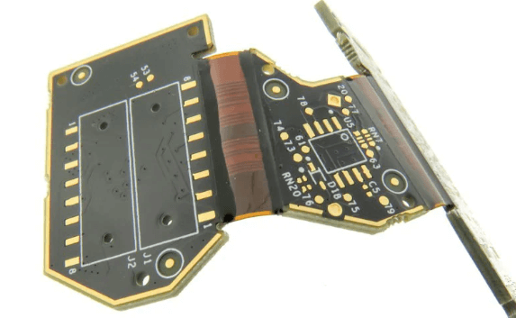
PCB locator hole requirements:
The PCB design industry has matured, and therefore, the requirements for PCB locator holes are very sophisticated. The locator hole requirements are as follows:
- At least two locator holes must be provided on the diagonals of the board.
- The standard diameter of the locating holes is 3.2mm ± 0.05mm.
- For boards of different company products, the following preferred diameters may be used: 2.8mm ± 0.05mm, 3.0mm ± 0.5mm, 3.5mm ± 0.5mm, and 4.5mm ± 0.5mm. For different boards of the same product (such as DT boards and PP boards for ZXJ10), if the PCB dimensions are the same, the location of the locating holes must also be consistent.
- The locating holes are bare holes, i.e., non-metallized through-holes (except for RF boards).
- If existing mounting holes (except for the clip mounting holes) meet the above requirements, there is no need to create additional locating holes.
Some common specifications and accuracy requirements for locating holes:
- The diameter tolerance of the locating holes is generally within 0.01mm. Large tolerances in the PCB fabrication room can result in poor probe contact and inaccurate alignment of the interface connector automatic insertion mechanism.
- Positioning Hole Diameter Requirements: Keep it below 3mm to prevent deformation of the positioning pins. Larger diameters are inconvenient to operate.
- Positioning Hole Diameter Requirements: Keep it at least 1mm from the PCB to minimize short circuits and damage to the product during installation.
- Positioning Hole Type: Positioning holes are generally mechanically controlled without copper sinking, which prevents contact with the circuit board and provides higher precision.
- Positioning Hole Layout: Positioning holes should be located at the four corners or diagonals of the PCBA to achieve multi-point surface positioning, ensuring precise positioning. The farther apart, the better.
- The distance between the positioning hole and the test point should be at least 2mm to prevent accidental short circuits during testing.
- The distance between the positioning hole and the board edge should be at least 2mm to ensure PCBA strength while preventing cracking.

