What are the manufacturing and process requirements of double-sided PCB?
In the following content, the editor will report the relevant news of double-layer PCB boards. If double-layer PCB boards are one of the focuses you want to know, you may wish to read this article with the editor.
1.Double-layer PCB boards
Both sides of double-sided PCB boards have wiring. However, to use the wires on both sides, there must be a proper circuit connection between the two sides. This “bridge” between circuits is called a via. A via is a small hole filled or coated with metal on the PCB, which can be connected to the wires on both sides.
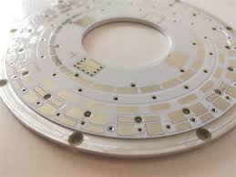
Double-sided boards are printed circuit boards with copper on both sides, including the Top (top layer) and the Bottom (bottom layer). They are the most common and most versatile circuit boards. Both sides of the insulating substrate have conductive patterns, and the electrical connections on both sides are mainly connected through vias or pads. Because both sides can be wired, the difficulty of wiring is greatly reduced, so it is widely used.
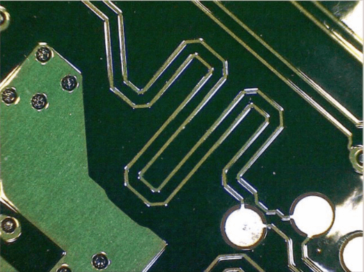
Both sides of the double-sided board have wiring, but to use the wires on both sides, there must be a proper circuit connection between the two sides, as shown in the figure. This kind of “bridge” between circuits is called a guide hole. A guide hole is a small hole filled or coated with metal on a PCB board, which can be connected to the wires on both sides. Because the area of a double-sided board is twice that of a single-sided board, a double-sided board solves the difficulty of wiring interlacing in a single-sided board (it can be connected to the other side through the hole), and it is more suitable for more complex circuits than a single-sided board.
The production method of a double-sided PCB is generally to make the inner layer graphics first, and then use the printing and etching method to make a single-sided or double-sided substrate, and incorporate it into the specified layer, and then heat, pressurize and bond it. As for the subsequent drilling, it is the same as the plated through hole method of the double-sided board. These basic production methods have not changed much from the methods dating back to the 1960s, but as the materials and process technologies (for example: press bonding technology, solving the glue residue generated during drilling, and the improvement of film) become more mature, the characteristics of the attached multi-layer board are more diverse.
2.What are the process requirements for double-layer PCB boards
In the modern electronic manufacturing industry, double-layer PCB boards are one of the basic types of circuit boards. Generally speaking, double-layer PCBs require not only fine craftsmanship, but also close coordination with the design of the circuit board to ensure production quality. The following will introduce the process requirements of double-layer PCBs.
(I) Boilerman
Boilermen play an important role in making double-layer PCBs. Boilermen need to be proficient in the physical and chemical properties of various materials and mix and process the raw materials according to the production process. The production process needs to consider factors such as thickness uniformity, adhesion and high temperature resistance. Therefore, boilermen should have good professional qualities and a high sense of responsibility.
(II) Plywood
During the plywood process, copper foil substrates, glass fiber cloth and other materials need to be combined to form a double-layer PCB, and ensure the surface flatness and thickness uniformity. After forming, pressure testing is also required to detect the degree of adhesion and compression strength between the various materials. Since double-layer PCBs need to bear the external force of electronic components and connecting wires, the bonding strength is very important.
(III) Gold plating is the process of depositing metal on copper foil.
After the metal is polarized, current is introduced from the power supply, and the metal ions are regenerated into metal in the electrolyte. In this process, it is necessary to ensure that the surface integrity and adhesion of the board meet the requirements, and at the same time, it is necessary to strictly control parameters such as inductance and resistance to achieve the best conductivity of the copper foil board.
(IV) Hole dripping
Hole dripping is a process applied after the double-layer PCB board is cut and the hole is pre-drilled. In this process, attention should be paid to the position, size and surface treatment of the hole to ensure the wire and communication quality of the hole.
(V) Filming
The double-layer PCB board needs to be laminated on the surface after cutting to protect the surface. At the same time, this technology can also provide different types of surface impedance and maintain high temperature performance. The quality of the composite process is affected by factors such as the quality and uniformity of the coating. In addition, it is necessary to ensure the corresponding process conditions and complete it under the guidance of the process documentation.
When making double-layer PCB boards, in addition to the above process requirements, it is also necessary to strictly control the process links such as cutting, drilling, and silver plating. During the production process, the process personnel need to carefully observe each process link, make timely adjustments and record the process to ensure the improvement of production quality and efficiency.
Finally, the editor sincerely thanks everyone for reading. Every time you read this article, it is a great encouragement and inspiration to me. I hope you have a preliminary understanding of double-layer PCB boards. Finally, I wish you all a wonderful day.