What are the simple and practical heat dissipation methods for PCBs?
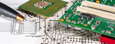
PCB (Printed Circuit Board), Chinese name for printed circuit board, also known as printed circuit board, is an important electronic component, a support for electronic components, and a carrier for electrical connection of electronic components. Because it is made by electronic printing, it is called a “printed” circuit board.
Function
After electronic equipment uses printed boards, due to the consistency of similar printed boards, manual wiring errors are avoided, and electronic components can be automatically inserted or mounted, automatically soldered, and automatically tested, ensuring the quality of electronic equipment, improving labor productivity, reducing costs, and facilitating maintenance.
Classification
(I) Single-Sided Boards
On the most basic PCB, the parts are concentrated on one side, and the wires are concentrated on the other side (the surface mount components are on the same side as the wires, and the plug-in components are on the other side
(II) Double-Sided Boards
Double-Sided Boards have wiring on both sides of the circuit board, but to use the wires on both sides, there must be a proper circuit connection between the two sides.
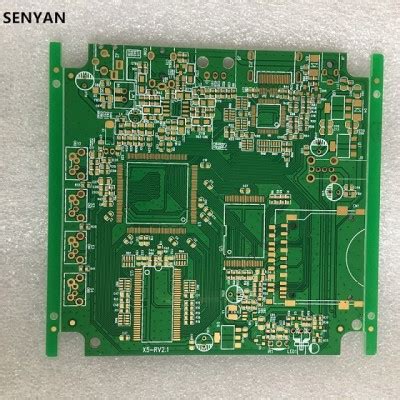
(III) Multi-Layer Boards
Multi-Layer Boards In order to increase the area that can be wired, multilayer boards use more single-sided or double-sided wiring boards.
10 PCB heat dissipation methods
PCB heat dissipation. For electronic devices, a certain amount of heat will be generated during operation, which will cause the internal temperature of the device to rise rapidly. If the heat is not dissipated in time, the device will continue to heat up, the device will fail due to overheating, and the reliability of the electronic equipment will decrease. Therefore, it is very important to perform good heat dissipation treatment on the circuit board. The heat dissipation of PCB circuit boards is a very important link, so what are the heat dissipation techniques of PCB circuit boards? Let’s discuss it together.
(I) Heat dissipation through the PCB board itself The currently widely used PCB board material is copper-clad/epoxy glass cloth substrate or phenolic resin glass cloth substrate, and a small amount of Paper-based copper-clad laminates are used.
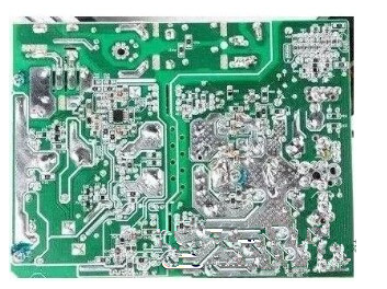
Although these substrates have excellent electrical and processing properties, they have poor heat dissipation. As a heat dissipation path for high-heat components, it is almost impossible to expect the PCB resin to conduct heat, but to dissipate heat from the surface of the component to the surrounding air. However, as electronic products have entered the era of miniaturization, high-density installation, and high-heat assembly, it is not enough to rely solely on the surface of components with very small surface areas to dissipate heat. At the same time, due to the large-scale use of surface-mounted components such as QFP and BGA, the heat generated by the components is transferred to the PCB board in large quantities. Therefore, the best way to solve the heat dissipation problem is to improve the heat dissipation capacity of the PCB itself that is in direct contact with the heat-generating components, and conduct or dissipate it through the PCB board
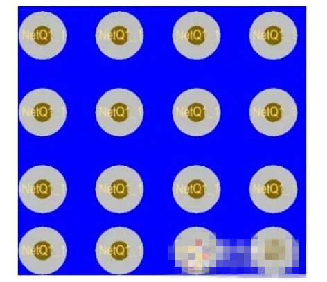
Add heat dissipation copper foil and use large-area power ground copper foil
Thermal vias
The copper on the back of the IC is exposed to reduce the copper skin Thermal resistance with air
PCB layout
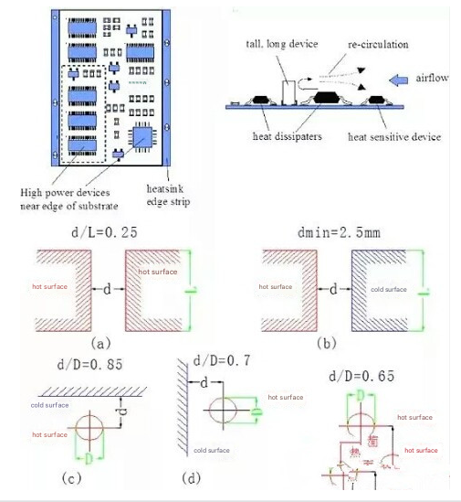
a. Heat-sensitive devices are placed in the cold air zone.
b. Temperature detection devices are placed in the hottest position.
c. Devices on the same printed circuit board should be arranged according to their heat generation and heat dissipation as much as possible. Devices with low heat generation or poor heat resistance (such as small signal transistors, small-scale integrated circuits, electrolytic capacitors, etc.) are placed at the uppermost stream (entrance) of the cooling airflow, and devices with high heat generation or good heat resistance (such as power transistors, large-scale integrated circuits, etc.) are placed at the lowest downstream of the cooling airflow.
d. In the horizontal direction, high-power devices are arranged as close to the edge of the printed circuit board as possible to shorten the heat transfer path; in the vertical direction, high-power devices are arranged as close to the top of the printed circuit board as possible to reduce the impact of these devices on the temperature of other devices when they are working.
e. The temperature of the printed circuit board in the equipment Heat dissipation mainly relies on air flow, so when designing, it is necessary to study the air flow path and reasonably configure the components or printed circuit boards. When air flows, it always tends to flow to places with low resistance, so when configuring components on a printed circuit board, avoid leaving a large airspace in a certain area. The same problem should also be noted when configuring multiple printed circuit boards in a whole machine.
f. Devices that are sensitive to temperature are best placed in the area with the lowest temperature (such as the bottom of the device). Never place it directly above the heating device. Multiple devices are best arranged in a staggered layout on the horizontal plane.
g. Arrange the devices with the highest power consumption and the highest heat generation near the best heat dissipation position. Do not place devices with higher heat generation in the corners and edges of the printed circuit board unless there is a heat dissipation device near it. When designing power resistors, choose larger devices as much as possible, and adjust them when adjusting. When the whole printed circuit board is laid out, there should be enough space for heat dissipation.
h. Component spacing recommendations:
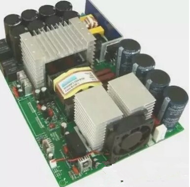
(ii) High-heat-generating components with heat sinks and heat conduction plates When there are a few components in the PCB that generate a lot of heat (less than 3), a heat sink or heat pipe can be added to the heat-generating components. When the temperature cannot be lowered, a heat sink with a fan can be used to enhance the heat dissipation effect.
When there are a large number of heat-generating components (more than 3), a large heat dissipation cover (plate) can be used. It is a special heat sink customized according to the position and height of the heat-generating components on the PCB board, or a large flat heat sink with different component heights cut out. The heat dissipation cover is buckled on the component surface as a whole, and it contacts each component to dissipate heat. However, due to the poor height consistency of components during soldering, the heat dissipation effect is not good. Usually, a soft thermal phase change thermal pad is added on the component surface to improve Heat dissipation effect.
(iii) For equipment using free convection air cooling, it is best to arrange the integrated circuits (or other devices) in a longitudinal or transverse manner.
(iv) Use reasonable routing design to achieve heat dissipation. Since the resin in the board has poor thermal conductivity, and the copper foil lines and holes are good conductors of heat, increasing the copper foil surplus rate and increasing the thermal conductive holes are the main means of heat dissipation. To evaluate the heat dissipation capacity of PCB, it is necessary to calculate the equivalent thermal conductivity (9eq) of the insulating substrate for PCB, a composite material composed of various materials with different thermal conductivities.
(v) The devices on the same printed circuit board should be arranged according to their heat generation and heat dissipation degree as much as possible. Devices with low heat generation or poor heat resistance (such as small signal transistors, small-scale integrated circuits, electrolytic capacitors, etc.) should be placed at the uppermost (entrance) of the cooling airflow. ), devices with high heat generation or good heat resistance (such as power transistors, large-scale integrated circuits, etc.) are placed at the downstream of the cooling airflow.
(vi) In the horizontal direction, high-power devices are arranged as close to the edge of the printed circuit board as possible to shorten the heat transfer path; in the vertical direction, high-power devices are arranged as close to the top of the printed circuit board as possible to reduce the impact of these devices on the temperature of other devices when they are working.
(vii) The heat dissipation of the printed circuit board in the equipment mainly depends on air flow, so when designing, the air flow path should be studied and the devices or printed circuit boards should be reasonably configured. When air flows, it always tends to flow to places with low resistance, so when configuring devices on the printed circuit board, avoid leaving a large airspace in a certain area. The same problem should also be paid attention to when configuring multiple printed circuit boards in the whole machine
(viii) Devices that are more sensitive to temperature are best placed in The lowest temperature area (such as the bottom of the device) should never be placed directly above the heating device. It is best to stagger multiple devices on the horizontal plane.
(IX) Place the devices with the highest power consumption and the highest heat generation near the best heat dissipation position. Do not place high-heat devices in the corners and edges of the printed circuit board unless there is a heat dissipation device near it. When designing power resistors, choose larger devices as much as possible, and make sure there is enough heat dissipation space when adjusting the printed circuit board layout.
(X) Avoid the concentration of hot spots on the PCB, distribute the power evenly on the PCB board as much as possible, and keep the PCB surface temperature performance uniform and consistent. It is often difficult to achieve strict uniform distribution during the design process, but it is necessary to avoid areas with too high power density to avoid overheating and affect the normal operation of the entire circuit.