What causes PCB leakage?
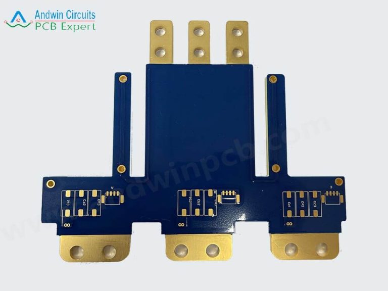
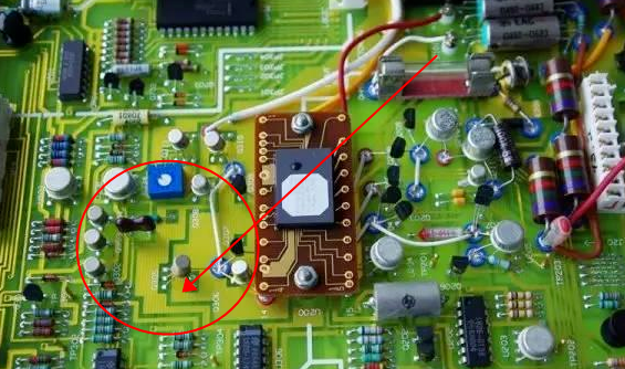
I recently encountered a PCB leakage issue with a low-power product. Originally, the device drew only µA current, but after a period of aging and use at room temperature, its power consumption increased, reaching the mA level in some prototypes. After carefully troubleshooting component issues, I finally discovered a 5V voltage point. While the device should be at 0V in sleep mode, it was experiencing a voltage drop of approximately 1.8V! Patiently cutting the PCB traces, I was surprised to discover that two vias, with no electrical connection at all, could measure hundreds of ohms of resistance between them. Examining the original design revealed a two-layer board with a via-to-pad spacing of >6 mils and a via-to-wall spacing of >18 mils—a typical drilling process in the PCB industry. After washing away the ink and eliminating any conductive impurities from the ink or the via surface, the resistance between the vias remained! After considerable puzzlement, I discovered the leakage was caused by the “CAF effect”!
What is the CAF effect?
CAF, short for Conductive Anodic Filamentation (CAF), refers to the leakage behavior of copper and copper salts within a PCB, which occurs when copper ions migrate from the anode (high voltage) along microcracks between glass fibers to the cathode (low voltage).
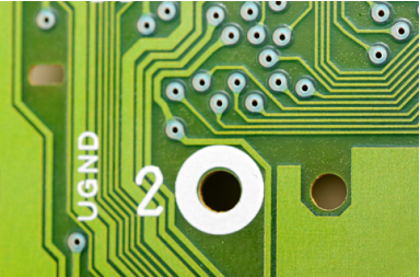
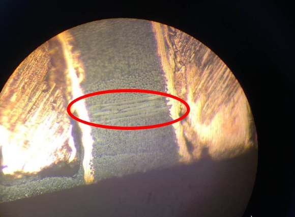
In the image below, two adjacent vias were milled longitudinally and magnified 100x under an electron microscope. The board appears dull in color, while the bright gold portion is copper. Copper dots and filaments can be seen between the two vias.
Mechanism of CAF:
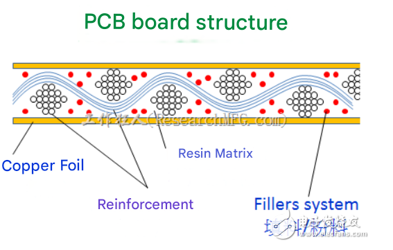
- Conventional FR4 PCBs are made by weaving glass fibers into a glass cloth, then coating them with epoxy resin and semi-curing them. Insufficient adhesion between the resin and the glass fibers, or poor adhesion during impregnation, can easily lead to gaps between the two. Furthermore, during machining processes like drilling, tangential tension and longitudinal impact forces further damage the resin’s bond, potentially causing the glass fiber bundles to loosen or separate, resulting in gaps. In high-temperature and high-humidity environments, the adhesion between epoxy resin and glass fiber deteriorates further, promoting chemical hydrolysis of the silane coupling agent on the glass fiber surface, creating pathways for electron migration along the glass fiber reinforcement.
- Based on the above conditions, if there is a potential difference between two closely spaced vias, the copper at the anode (with a higher potential) will be oxidized into copper ions. Under the influence of the electric field, the copper ions migrate toward the cathode (with a lower potential). During this migration, they combine with impurity ions or OH-ions in the board, forming water-insoluble conductive salts that are deposited. This causes a sharp decrease in the electrical spacing between the two insulating vias, and in severe cases, can even lead to direct conduction, resulting in a short circuit.
Anode:
Cu → Cu2++2e–
H2O → H++OH–
Cathode:
2H++2e– → H2
Cu2++2OH– → Cu(OH)2
Cu(OH)2 → CuO+H2O
CuO+H2O → Cu(OH)2 → Cu2++2OH–
Cu2++2e– → Cu
Before I realized the potential for CAF to cause defects, I was amazed by the resistance between two insulated vias. Later, after researching, I discovered that many of my colleagues had also struggled with this issue, and that the CAF effect has become a major reliability issue in the PCB industry!
How to prevent or reduce CAF?
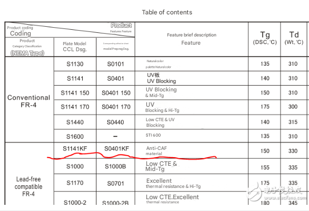
- Improve the board’s CAF resistance. For PCB substrate processing, improvements can be made by increasing the ionic purity of the material, using low-hygroscopic resins, and ensuring that the glass cloth is fully impregnated and bonded to the resin. Application engineers can consider using CAF-resistant board materials when selecting board materials. For example, the following board supplier, Shengyi, offers CAF-resistant boards.
- Mechanical drilling or laser burning of PCBs generates high temperatures. When the temperature exceeds the Tg point of the board, it melts and forms residue. This residue adheres to the hole walls, causing poor contact during copper plating. Therefore, deslagging is necessary before copper plating. The soaking treatment during deslagging can cause some corrosion to the through-holes and may cause copper seepage, making subsequent copper migration more likely.
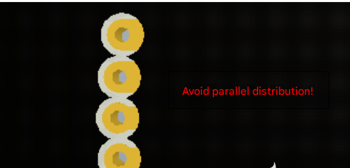
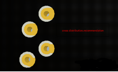
- During PCB design, increase the spacing between through-holes. Additionally, since CAF channels typically form along the same fiberglass strands, interleaving adjacent through-holes can help reduce CAF.
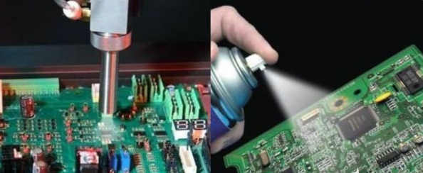
- Clean the PCBA surface, such as using a high-pressure air gun to remove dust, to prevent residual impurities from electrolyzing unwanted impurities. Additionally, apply conformal coating to the PCBA surface to prevent moisture intrusion, especially in high-temperature and high-humidity environments.
Regarding this leakage issue caused by CAF, from initial confusion to subsequent enlightenment, two key insights have deepened my understanding:
- When faced with a bug, even when you find yourself baffled, maintain an objective attitude. The phenomenon is often far from what you already know, and it’s likely simply a blind spot in your knowledge. When I encountered CAF, I posed the question to the PCB manufacturer, “Why is there resistance between mutually insulated vias?” The manufacturer also found it baffling, but based on their empirical understanding that they had never encountered this issue in decades of board manufacturing, they failed to objectively address the issue. Under these circumstances, even with the best cooperation, so-called verification can only be limited to self-certification of materials and processes that meet industry standards. However, CAF is a problem that cannot be completely avoided in the current PCB industry. This forced me to consult a third-party manufacturer for cross-section analysis. After clearly seeing the copper between the vias, the issue was finally resolved with irrefutable certainty.
- Application-side electronic engineers, in addition to being able to use and master electronic components, also need to have a basic understanding of their materials. We work with components like capacitors, resistors, and inductors every day, but many people are unaware of their manufacturing processes and underlying material composition, which are the very foundation of their electrical properties. For example, why does a capacitor have resistive, inductive, and capacitive components at different operating frequencies? Or why does an aluminum electrolytic capacitor explode when reverse-connected? Is it guaranteed to explode if the reverse voltage is unknown? I’ll document and share these questions later.