What does PCB package library mean?
In the entire PCB copy board industry, the role of PCB is undoubtedly to carry the bridge connecting various electronic components, so the chip board has the “mother of electronic products” and is an indispensable part of the current electronic information products. After all, it is a type of electronic components, and PCB packaging plays a connecting role in the entire circuit board industry. Here, many friends will ask what PCB packaging means?
Nowadays is an era of 5G network construction and an era of big data.
We are surrounded by various artificial intelligence, new energy vehicles, and the Internet of Things. In such a rapidly developing era, the PCB industry has undoubtedly become an indispensable part of the entire electronic industry chain, and it plays a bearing role in the electronic industry chain. However, China’s current chip development is still some distance away from international development, so when we are self-reliant, we have been working hard.
What does PCB packaging mean?
PCB packaging is to express various parameters of actual electronic components, chips, etc. (such as the size of components, length and width, direct insertion, patch, pad size, length and width of pins, pin spacing, etc.) in a graphical way so that they can be called when drawing PCB diagrams. At present, PCB packaging is an integral part of the circuit board industry.
At present, the PCB industry is mainly distributed in Europe, America, Japan, South Korea, mainland China, Taiwan, China and other regions. Before 2000, the three major regions of America, Europe and Japan accounted for more than 70% of the global PCB production output value, but in the past decade, due to the advantages of population, resources, policies, and industrial agglomeration, the global electronic manufacturing capacity has shifted to Asian regions such as mainland China, Taiwan, China and South Korea. Since 2006, China has surpassed Japan to become the world’s largest PCB producer, with PCB production and output value ranking first in the world, gradually occupying half of the global PCB market.
Let’s predict the future of the PCB industry based on the present.
You must know that China, as the largest producer of the global PCB industry, currently accounts for 31.18% of the total output value of the global PCB industry, which has increased from 31.18% in 2008 to 54.22% in 2021. Authoritative data predicts that in the next five years, China will still be the world’s No. 1 PCB industry output value, and will continue to develop at a higher level than the global overall growth rate. Based on China’s huge domestic demand market and perfect supporting industrial chain, it can be expected that the trend of global PCB industry capacity transfer to China will continue for a long time in the future. The vast market space and stable growth rate provide rare development opportunities for my country’s industry participants.
What does PCB packaging mean?
After understanding the development trend of PCB and being familiar with the concept of PCB packaging, the development of this industry is also very clear. The industry is gradually tending towards high-end, mature and diversified development momentum, and PCB production and packaging work in China is further moving towards the mid-to-high-end market and extending vertically to this market. What does PCB packaging mean? Engineers from Dongguan Boyuan Electronics Co., Ltd. pointed out that now, with the continuous advancement of current process technology, many industries need to use PCB packaging, and good quality PCB packaging has even appeared in a market state of supply and demand. And we can also clearly know from the above content that the future development of PCB proofing will definitely be increasingly prosperous, and the development space is even more unfathomable.
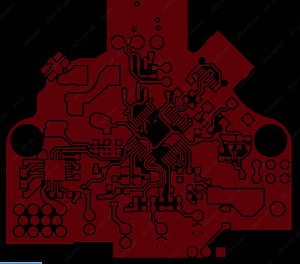
- Create a PCB library file: Click the “File” menu, select the “Library” option in the “New” option, and then select “PCB Library” to enter the editing interface of the component PCB package. 2. Save the PCB library file: Select the “File” menu, select the “Save As…” option, name the file “Package Library” and save it.
- The operation interface of the PCB library component is similar to the PCB editing interface, including zooming in and out of the view, moving and flipping components, etc. Note that in the operation interface of the library component, a single component is edited, not the entire PCB diagram, and the component must be placed near the coordinate origin for editing. Operation to find the origin: Edit->Jump->Reference
- Modify the properties of the editing interface: Click the mouse cursor in the “Properties” editing window on the right. Common settings are: “Grid Manager-> Properties->Step->Step X” option “X” and “Y” can set the minimum moving distance of the horizontal and vertical coordinates of the mouse movement, respectively, according to the specific size of the component; “Other->Unit” option can modify the unit used (“mils” option is milliinches as the unit, “mm” option is millimeters as the unit);
- Make direct plug components (take the SMA component in the figure below as an example), SMA-KE package (the right is the actual picture). Enlarge the window to a suitable position (see the grid), select the “Pad” option under the “Place” menu to place a pad, then the mouse cursor becomes a movable pad, use the “Ctrl+End” key combination to automatically move the pad to the coordinate origin, and click the left button to confirm the placement.
- Modify the pad properties: Double-click the pad, and the “Properties” modification interface will pop up in the right window. The “Properties-> Designator” option can change the pad number; the “Layer” option can change the pad layer (if it is a plug-in component, select “Multi-Layer”, if it is a patch component, select the top layer “Top Layer” or the bottom layer “Bottom Layer”); the “X-Size” and “Y-Size” options modify the horizontal coordinate width and vertical coordinate height of the pad respectively; the “Hole information->Hole Size” item can modify the diameter of the inner hole of the pad; the “Round” option can make the shape of the inner hole a round hole; the “Rect” option can make the shape of the inner hole a square hole. When this item is selected, the “Rotation” option can enter the rotation angle of the inner hole; the “Slot” option can make the shape of the inner hole an elliptical hole. When this item is selected, the “Rotation” option can enter the rotation angle of the inner hole. The “Length” option can enter the length of the ellipse (Note: the value of this item must be greater than the value of the inner hole diameter “Hole Size”); “Size and Shape-> “Shape” option to modify the shape of the pad (“Round” for round, “Rectangular” for square, “Octagonal” for octagon, “Rounded Rectangle” for rounded square), X/Y is used to modify the size of the pad. Other parameters do not need to be modified.
- According to the above content, set the parameters of the placed pad as follows: the inner hole is a round hole with a diameter of 1.2mm, the pad number is 1, and the pad is a 2.2mm×2.2mm round pad.
PCB packaging is to express various parameters of actual electronic components, chips, etc.: the size, length and width of electronic components, direct insertion, patch, pad size, pin length and width, pin spacing, etc., in a graphical way, so that it can be called when drawing PCB diagrams.
PCB packaging can be divided into: mounted devices, plug-in devices, mixed devices, special devices (sunken board devices) according to the installation method

So what are the common forms of PCB packaging?
Spherical contact display, one of the surface mount type packaging. Spherical bumps are made on the back of the printed circuit board in an array to replace the pins, and the LSI chip is assembled on the front of the printed circuit board, and then sealed with molded resin or potting. It is also called a bump array carrier (PAC). The number of pins can exceed 200, which is a package for multi-pin LSI. The package body can also be made smaller than QFP (quad flat package). For example, a 360-pin BGA with a pin center distance of 1.5mm is only 31mm square; while a 304-pin QFP with a pin center distance of 0.5mm is 40mm square. Moreover, BGA does not have to worry about the pin deformation problem like QFP.
This package was developed by Motorola in the United States and was first adopted in portable phones and other devices. It is likely to be popularized in personal computers in the United States in the future. Initially, the pin (bump) center distance of BGA was 1.5mm and the number of pins was 225. Now some LSI manufacturers are also developing 500-pin BGA. The problem with BGA is the appearance inspection after reflow soldering. It is not clear whether there is an effective appearance inspection method. Some people think that due to the large center distance of the soldering, the connection can be regarded as stable and can only be handled by functional inspection. Motorola in the United States calls the package sealed with molded resin OMPAC, and the package sealed by potting method GPAC (see OMPAC and GPAC).
There are three main elements to pay attention to when making a component package:
- Pads – used to fix the device to the circuit board and connect signals with other devices through wires. We need to draw the shape, position and pad number of the device according to the data sheet. The number corresponds to the pin number of the device;
- Outline – The outline of the component package is to tell the designer the area occupied by the device. No device can be placed within the outline, otherwise it will cause a conflict;
- Silkscreen marking – We need to mark the key information of the device through silkscreen, such as which pin is the starting pin? The polarity and direction of the device, etc. In addition to the above three elements, most CAD software has added 3D data. Based on these data, designers can know the three-dimensional shape of the device, which is very important in mechatronic design.