What is a 4-Layer PCB? Understanding Four-Layer, Single-Step Printed Circuit Boards
Introduction to Multi-Layer PCBs
Printed Circuit Boards (PCBs) form the backbone of modern electronics, providing the physical platform for component mounting and electrical connections between parts. As electronic devices have become more complex while shrinking in size, the demand for multi-layer PCBs has grown exponentially. Among these, the 4-layer PCB has emerged as one of the most popular configurations, offering an optimal balance between complexity, cost, and performance for many applications.
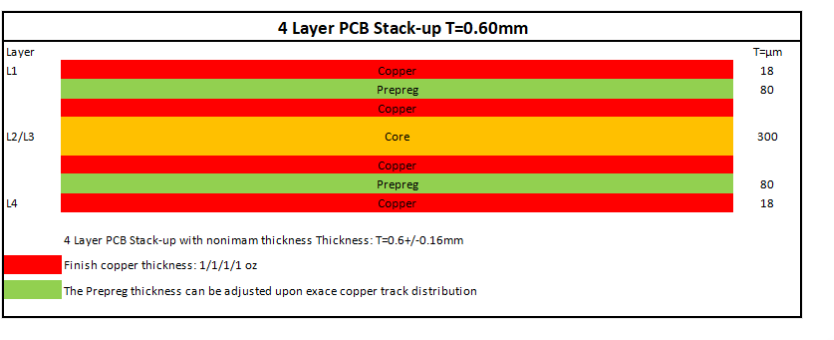
A 4-layer PCB, as the name suggests, consists of four conductive copper layers laminated together with insulating material in between. These boards represent a significant step up from simple single or double-sided boards while avoiding the excessive complexity and cost of higher-layer-count solutions. The “single-step” or “one-step” designation refers to a specific manufacturing approach where all layers are processed simultaneously rather than in sequential steps, offering certain production advantages.
Structure of a 4-Layer PCB
The standard architecture of a 4-layer PCB follows a specific layer stack-up that has become an industry convention:
- Top Layer (Signal Layer): The outermost layer where most components are mounted and where high-speed signals typically run.
- Inner Layer 1 (Ground Plane): A solid copper plane connected to ground, providing shielding and a stable reference for signals.
- Inner Layer 2 (Power Plane): A solid copper plane dedicated to power distribution, often split for multiple voltage levels.
- Bottom Layer (Signal Layer): The opposite outer layer used for additional component placement and signal routing.
This sandwich-like construction provides several advantages over 2-layer boards. The internal power and ground planes create a low-impedance power distribution network while offering inherent electromagnetic interference (EMI) shielding. The separation between signal layers reduces crosstalk, and the overall design allows for higher component density.
Manufacturing Process of Single-Step 4-Layer PCBs
The production of 4-layer PCBs can follow either sequential build-up or single-step (one-step) processes. The single-step method, while requiring more sophisticated equipment, offers several manufacturing benefits:
- Material Preparation: All four copper-clad laminate cores are prepared simultaneously.
- Inner Layer Processing: Inner layers (2 and 3) are patterned and etched in parallel.
- Alignment and Lamination: All layers are aligned using registration holes and laminated together in one pressing operation.
- Drilling: Through-holes are drilled after lamination, penetrating all layers at once.
- Plating and Outer Layer Processing: The entire stack receives plating and outer layer patterning in unified steps.
This approach contrasts with sequential build-up methods where layers might be added one at a time. The single-step process typically results in better layer-to-layer registration, reduced production time, and potentially lower costs for volume production.
Advantages of 4-Layer PCBs
The transition from 2-layer to 4-layer designs offers numerous benefits that explain their widespread adoption:
- Improved Signal Integrity: The presence of uninterrupted ground and power planes provides consistent reference planes for high-speed signals, reducing noise and reflections.
- Better Power Distribution: Dedicated power planes offer low-impedance paths for power delivery, minimizing voltage drops across the board.
- Enhanced EMI Performance: The sandwich structure naturally contains electromagnetic fields, reducing both emissions and susceptibility to interference.
- Increased Routing Density: With four layers available, complex designs can be routed without excessive via usage or trace crowding.
- Thermal Management: The additional copper mass helps dissipate heat more effectively than thinner boards.
- Size Reduction: Equivalent functionality can often be achieved in a smaller footprint compared to 2-layer solutions.
Design Considerations for 4-Layer PCBs
Effective utilization of a 4-layer stack-up requires careful planning:
- Layer Assignment Strategy: Determine which signals will go on which layers early in the design process.
- Impedance Control: Calculate trace widths to achieve target impedances based on the dielectric materials used.
- Via Selection: Choose appropriate via types (through-hole, blind, or buried) based on signal requirements.
- Power Plane Segmentation: If multiple voltages are needed, plan power plane splits carefully to avoid creating antenna structures.
- Signal Layer Routing Direction: Alternate primary routing directions between top and bottom layers to minimize crosstalk.
- Decoupling Capacitor Placement: Optimize placement to take full advantage of the power plane structure.
Applications of 4-Layer PCBs
The versatility of 4-layer PCBs makes them suitable for a wide range of applications:
- Consumer Electronics: Smartphones, tablets, and wearable devices often use 4-layer boards for their compact size and good signal integrity.
- Networking Equipment: Routers, switches, and communication devices benefit from the EMI performance and routing density.
- Industrial Controls: Reliable power distribution is critical for industrial automation systems.
- Automotive Electronics: The robust construction suits the demanding automotive environment.
- Medical Devices: Where reliability and signal integrity are paramount.
- IoT Products: Combining compact size with adequate complexity for smart devices.

Cost Considerations
While 4-layer PCBs cost more than 2-layer versions, the single-step manufacturing process helps control expenses. The actual price premium depends on:
- Board Size: Larger boards see a smaller percentage increase compared to 2-layer.
- Material Choices: High-frequency or specialized materials add cost regardless of layer count.
- Volume: The single-step process becomes more economical at higher quantities.
- Design Complexity: Features like blind/buried vias or tight tolerances increase cost.
In many cases, the system-level savings from reduced size, improved reliability, and better performance justify the additional PCB cost.
Comparison with Other Layer Counts
Understanding where 4-layer fits in the PCB hierarchy helps with technology selection:
- vs 2-Layer: 4-layer offers better performance and density but at higher cost.
- vs 6-Layer: 6-layer provides more routing channels but with significantly higher cost and potentially longer lead times.
- vs 8+ Layer: High-layer-count boards enable extreme complexity but require advanced design skills and carry premium pricing.
For many applications, 4-layer represents the sweet spot between capability and affordability.
Future Trends in 4-Layer PCB Technology
The 4-layer PCB continues to evolve with several emerging trends:
- Higher Density Interconnects: Finer trace/space capabilities allow more functionality per unit area.
- Advanced Materials: New dielectric materials offer better high-frequency performance.
- Embedded Components: Passive components integrated within the PCB layers.
- Improved Thermal Management: Novel materials and structures for heat dissipation.
- Design Automation Tools: More sophisticated software for optimizing 4-layer layouts.
Conclusion
The 4-layer single-step PCB represents a crucial technology in modern electronics manufacturing, offering an optimal balance between performance, complexity, and cost. Its standardized layer stack-up provides inherent advantages for signal integrity, power distribution, and EMI control that make it the go-to solution for countless applications. As electronic devices continue advancing, the 4-layer PCB will remain a fundamental building block, with ongoing improvements in materials and manufacturing processes ensuring its relevance for years to come. Understanding its structure, benefits, and proper design techniques is essential for engineers developing today’s electronic products.