What is a PCB Stencil and What Are Its Functions?
Introduction to PCB Stencils
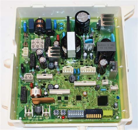
In the world of printed circuit board (PCB) manufacturing and assembly, precision and efficiency are paramount. One critical tool that enables both is the PCB stencil, commonly referred to as a “PCB steel stencil” or simply “PCB stencil.” This specialized tool plays a vital role in the surface mount technology (SMT) assembly process, ensuring accurate and consistent application of solder paste onto PCB pads.
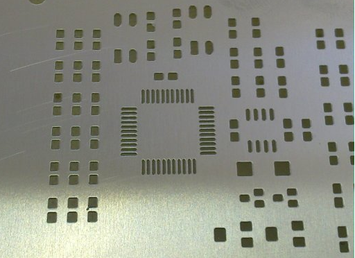
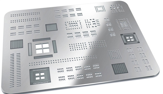
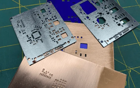
A PCB stencil is essentially a thin sheet of material (typically stainless steel) with precisely cut openings that correspond to the solder pad locations on a PCB. When aligned properly over a PCB, the stencil allows solder paste to be deposited exactly where needed for component placement. The stencil’s design and quality directly impact the solder paste deposition’s accuracy, which in turn affects the overall quality of the solder joints and the reliability of the final electronic assembly.

Types of PCB Stencils
1. Laser-Cut Stencils
The most common and precise type, laser-cut stencils are created using high-powered lasers that vaporize material to form the apertures. This method offers excellent precision (typically ±0.025mm or better) and can produce very fine pitch patterns suitable for modern high-density PCB designs.
2. Electroformed Stencils
These stencils are created through an electroforming process where nickel is deposited onto a mandrel to form the stencil. Electroformed stencils offer superior smoothness on aperture walls, which improves solder paste release characteristics, making them ideal for ultra-fine pitch applications.
3. Chemical-Etched Stencils
Created through a chemical etching process, these stencils are more economical but less precise than laser-cut versions. The etching process can create slightly tapered apertures, which may be beneficial for certain applications but generally offer lower precision (±0.075mm or more).
4. Hybrid Stencils
Combining different manufacturing techniques, hybrid stencils might use laser-cutting for most apertures but electroforming for particularly challenging areas, offering a balance between cost and performance.
5. Framed vs. Frameless Stencils
Framed stencils are permanently mounted in a metal frame for stability and ease of use, while frameless stencils are more flexible and typically used with reusable tensioning systems.
Materials Used in PCB Stencils
1. Stainless Steel
The most common material (typically 300 or 400 series) due to its excellent durability, stability, and resistance to wear. Stainless steel stencils can withstand thousands of printing cycles while maintaining dimensional stability.
2. Nickel
Used primarily in electroformed stencils, nickel offers very smooth aperture walls and can be plated to specific thicknesses with high precision.
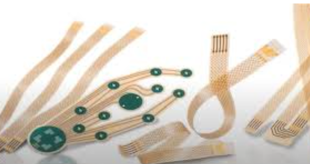
3. Polyimide (Kapton)
Plastic stencils used for prototyping or low-volume production. While less durable than metal stencils, they are cheaper and quicker to produce.
4. Mylar
Another plastic material sometimes used for temporary or prototype stencils, though with significant limitations in precision and durability.
Key Functions of PCB Stencils
1. Precise Solder Paste Deposition
The primary function of a PCB stencil is to deposit the correct amount of solder paste onto each PCB pad with high precision. The stencil ensures that:
- Solder paste is applied only where needed
- The correct volume of paste is deposited for each component
- Paste is accurately aligned with the underlying pads
2. Controlling Solder Volume
The stencil thickness and aperture design directly control the amount of solder paste deposited:
- Standard stencils are typically 0.1-0.15mm thick for standard components
- Thinner stencils (0.08mm or less) may be used for fine-pitch components
- Thicker stencils (up to 0.2mm) might be used for large components requiring more solder
3. Enabling High-Speed Assembly
PCB stencils allow for rapid, consistent application of solder paste across an entire board in a single step, enabling high-speed SMT assembly lines to maintain throughput.
4. Supporting Various Component Types
Modern stencils can accommodate:
- Standard SMT components (resistors, capacitors, ICs)
- Fine-pitch components (down to 0.3mm pitch or less)
- Ball grid array (BGA) packages
- Quad flat no-lead (QFN) packages
- Large components like connectors or power devices
5. Facilitating Process Consistency
By providing a consistent method for solder paste application, stencils help maintain process control and reduce variability in the soldering process.
Stencil Design Considerations
1. Aperture Design
The shape and size of stencil apertures significantly affect solder paste deposition:
- Apertures are typically slightly smaller than the pad (90-95% area ratio for good release)
- Special shapes (home plate, rounded corners) can improve paste release
- Aspect ratio (aperture width/stencil thickness) should typically be >1.5
- Area ratio (aperture area/aperture wall area) should typically be >0.66
2. Stencil Thickness
Thickness selection depends on:
- Component types and sizes on the PCB
- Required solder volume for each joint
- Fine-pitch component requirements
- Often involves compromises between different component needs
3. Step Stencils
Some designs use varying thicknesses across the stencil:
- Step-down areas for fine-pitch components
- Step-up areas for components needing more solder
- Allows optimization for mixed-technology boards
4. Fiducial Marks
Alignment marks that help ensure proper registration between the stencil and PCB.
5. Nano-Coating
Some stencils receive special coatings to improve solder paste release and reduce cleaning frequency.
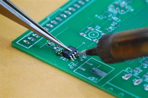
The PCB Stencil Printing Process
1. Stencil Alignment
The stencil is precisely aligned with the PCB using fiducial marks and mechanical alignment systems.
2. Solder Paste Application
Solder paste is applied to the stencil surface, typically using an automated squeegee system.
3. Printing
The squeegee blades move across the stencil, forcing solder paste through the apertures onto the PCB pads.
4. Separation
The stencil is carefully separated from the PCB, leaving precise deposits of solder paste.
5. Inspection
Automated optical inspection (AOI) systems often check the quality of the solder paste deposits.
Advantages of Using PCB Stencils
1. High Precision
Modern stencils can achieve extremely precise solder paste deposition, essential for today’s high-density PCB designs.
2. Consistency
Stencils provide consistent results across thousands of printing cycles when properly maintained.
3. Speed
Stencil printing is much faster than manual solder paste application methods.
4. Cost-Effectiveness
While requiring initial investment, stencils reduce labor costs and improve yield in volume production.
5. Flexibility
Stencil designs can be customized for specific PCB layouts and component requirements.
Common Challenges and Solutions
1. Solder Paste Release Issues
- Problem: Paste sticks to aperture walls instead of transferring to PCB
- Solutions: Improve aperture design, use nano-coatings, optimize squeegee parameters
2. Poor Alignment
- Problem: Misregistration between stencil apertures and PCB pads
- Solutions: Improve fiducial marking, enhance alignment systems, verify stencil design
3. Solder Bridging
- Problem: Excess solder causing shorts between adjacent pads
- Solutions: Adjust stencil thickness, modify aperture designs, optimize printing parameters
4. Insufficient Solder
- Problem: Incomplete or weak solder joints due to insufficient paste
- Solutions: Increase aperture sizes, use step stencils, verify paste quality
Maintenance and Care of PCB Stencils
Proper maintenance extends stencil life and ensures consistent performance:
- Regular cleaning to remove solder paste residue
- Proper storage to prevent damage or deformation
- Periodic inspection for wear or damage
- Careful handling to avoid bending or scratching
Future Trends in PCB Stencil Technology
1. Advanced Materials
Development of new alloys and coatings to improve release characteristics and durability.
2. Smart Stencils
Integration of sensors to monitor paste deposition and stencil wear in real-time.
3. 3D Printing
Potential for additive manufacturing to create complex stencil geometries not possible with traditional methods.
4. Adaptive Apertures
Research into apertures that can dynamically adjust size based on component requirements.
5. Enhanced Coatings
New nano-coatings that further improve paste release and reduce cleaning requirements.
Conclusion
PCB stencils are indispensable tools in modern electronics manufacturing, bridging the gap between PCB design and reliable assembly. Their precise control over solder paste deposition directly impacts product quality, manufacturing yield, and production efficiency. As electronic components continue to shrink and PCB designs grow more complex, the role of advanced stencil technology becomes even more critical. Understanding stencil types, materials, design considerations, and proper usage techniques enables manufacturers to optimize their SMT processes and produce high-quality electronic assemblies consistently.
The evolution of stencil technology continues to parallel advancements in electronics manufacturing, with new materials, manufacturing techniques, and design approaches constantly emerging to meet the challenges of next-generation PCB assembly. Whether for prototyping or high-volume production, selecting and implementing the appropriate PCB stencil solution remains a fundamental aspect of successful electronics manufacturing.