What is a PCB Stencil and What Are Its Functions?
Introduction
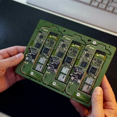
Printed Circuit Boards (PCBs) are essential components in modern electronics, serving as the foundation for mounting and interconnecting electronic components. One crucial tool in the PCB assembly process is the PCB stencil, also known as a solder paste stencil or steel mesh. This article explores what a PCB stencil is, its types, manufacturing processes, and its critical role in Surface Mount Technology (SMT) assembly.
1. What is a PCB Stencil?
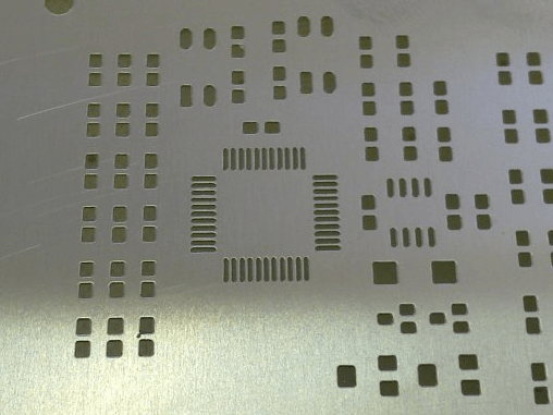
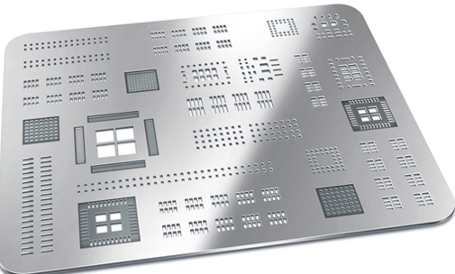
A PCB stencil is a thin sheet (typically made of stainless steel or polyimide) with precisely cut openings that correspond to the solder pad locations on a PCB. It is used to apply solder paste accurately onto the PCB before placing surface-mount components. The stencil ensures that the right amount of solder paste is deposited in the correct positions, enabling reliable electrical connections during reflow soldering.
Key Characteristics of PCB Stencils
- Material: Most stencils are made of stainless steel due to its durability and precision. However, some flexible stencils use polyimide (Kapton) for prototyping.
- Thickness: Typically ranges from 0.1 mm to 0.2 mm (4 to 8 mils), depending on component pitch and solder paste requirements.
- Aperture Design: The openings (apertures) are laser-cut or chemically etched to match PCB pad layouts.
2. Types of PCB Stencils
Different PCB stencil types are used based on assembly requirements:
(1) Laser-Cut Stencils
- Made using laser cutting technology for high precision.
- Suitable for fine-pitch components (e.g., BGA, QFN, 0201 resistors).
- Smooth aperture walls reduce solder paste clogging.
(2) Electroformed Stencils
- Created via electroplating nickel over a mandrel with the desired pattern.
- Extremely precise, with smooth walls for ultra-fine pitch components.
- More expensive than laser-cut stencils.
(3) Chemical Etched Stencils
- Produced by etching stainless steel sheets using acid.
- Cost-effective but less precise than laser-cut stencils.
- Suitable for larger components and prototypes.
(4) Framed vs. Frameless Stencils
- Framed stencils are mounted on a metal frame for stability in automated SMT machines.
- Frameless stencils (also called “prototype stencils”) are flexible and used for manual solder paste application.
3. How is a PCB Stencil Made?
The manufacturing process involves several steps:
- Design Preparation
- The PCB design file (Gerber or CAD data) is used to define stencil aperture locations.
- Stencil thickness and aperture dimensions are optimized for solder paste release.
- Material Selection
- Stainless steel (commonly 304 or 316 grade) is chosen for durability.
- Laser Cutting or Etching
- A laser-cutting machine precisely cuts apertures based on the PCB design.
- For etched stencils, a chemical process removes unwanted material.
- Surface Treatment (Optional)
- Electropolishing smoothens aperture walls to improve solder paste release.
- Nano-coating prevents solder paste sticking.
- Quality Inspection
- The stencil is checked for aperture accuracy, smoothness, and alignment.
4. Key Functions of PCB Stencils in SMT Assembly
PCB stencils play a vital role in ensuring high-quality solder joints and efficient PCB assembly. Their primary functions include:
(1) Precise Solder Paste Deposition
- The stencil ensures that solder paste is applied only to designated pads, preventing bridging or insufficient solder.
(2) Consistent Solder Volume Control
- The stencil thickness and aperture size determine the amount of solder paste deposited.
- Fine-pitch components require thinner stencils (e.g., 0.1 mm) to avoid excess solder.
(3) Improved SMT Assembly Efficiency
- Automated stencil printers enable high-speed, repeatable solder paste application, reducing manual errors.
(4) Support for Miniaturized Components
- Modern PCBs use tiny components like 01005 resistors and micro-BGAs, requiring ultra-precise stencils.
(5) Reduced Solder Defects
- Proper stencil design minimizes issues like:
- Solder bridging (excess solder causing shorts).
- Insufficient solder (weak joints).
- Solder balling (contamination due to improper paste release).
5. Common PCB Stencil Design Considerations
To optimize stencil performance, engineers follow these guidelines:
(1) Aperture Size and Shape
- Aperture width should be slightly smaller than the PCB pad to prevent bridging.
- Round or square apertures are common, but home-plate shapes improve paste release for fine-pitch parts.
(2) Stencil Thickness Selection
- Standard components: 0.12–0.15 mm (5–6 mils).
- Fine-pitch ICs: 0.08–0.1 mm (3–4 mils).
- Large power components: 0.2 mm (8 mils).
(3) Step-Up/Step-Down Stencils
- Some PCBs require different stencil thicknesses in certain areas (e.g., thicker paste for QFNs, thinner for BGAs).
(4) Fiducial Marks and Alignment
- Stencils include fiducial marks to align perfectly with the PCB.
6. Challenges and Solutions in PCB Stencil Usage
| Challenge | Solution |
|---|---|
| Solder paste clogging | Use electropolished or nano-coated stencils. |
| Poor paste release | Optimize aperture design (tapered walls). |
| Misalignment | Ensure accurate fiducial marks on PCB and stencil. |
| Stencil wear | Use high-quality stainless steel and proper cleaning. |
7. Conclusion
PCB stencils are indispensable in modern electronics manufacturing, enabling high-precision solder paste application for reliable SMT assembly. By selecting the right stencil type, thickness, and design, manufacturers can reduce defects, improve yield, and support advanced PCB technologies. As components continue to shrink, advancements in laser-cut and electroformed stencils will further enhance assembly accuracy and efficiency.
Key Takeaways
✔ PCB stencils ensure accurate solder paste deposition on PCBs.
✔ Laser-cut stencils are the most common for high-precision applications.
✔ Stencil thickness and aperture design impact solder joint quality.
✔ Proper stencil maintenance (cleaning, inspection) extends its lifespan.
By understanding PCB stencil technology, engineers and manufacturers can optimize their assembly processes for higher reliability and performance.