What is a solder mask opening?
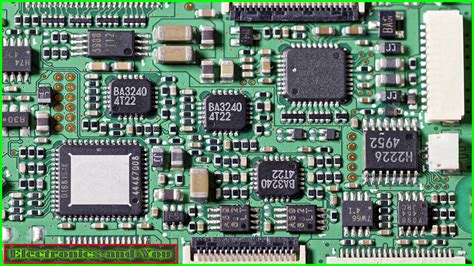
The solder mask is the soldermask, which refers to the part of the printed circuit board that is to be painted with green oil. In fact, this solder mask uses a negative output, so after the shape of the solder mask is mapped to the board, it is not the green oil solder mask that is applied, but the copper skin is exposed.
Process requirements for solder mask
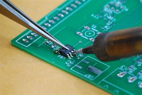
The role of the solder mask in controlling soldering defects during the reflow soldering process is important, and PCB designers should try to minimize the spacing or air gap around the pad features.
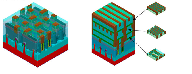
Although many process engineers would rather separate all the pad features on the board with a solder mask, the pin spacing and pad size of fine-pitch components will require special consideration. Although unpartitioned solder mask openings or windows on four-sided QFPs may be acceptable, it may be more difficult to control solder bridges between component pins. For the solder mask of BGA, many companies provide a solder mask that does not touch the pads, but covers any features between pads to prevent solder bridges. Most surface mount PCBs are covered with solder mask, but solder mask application, if thicker than 0.04mm (“), may affect solder paste application. Surface mount PCBs, especially those using fine pitch components, require a low profile photosensitive solder mask.
Processing of Solder Mask
Solder mask materials must be applied by either a liquid wet process or a dry film laminate. Dry film solder mask materials are supplied in 0.07-0.1mm (0.03-0.04″) thicknesses, which can be suitable for some surface mount products, but this material is not recommended for fine pitch applications. Few companies offer dry films thin enough to meet fine pitch standards, but several companies can provide liquid photosensitive solder mask materials. Typically, the solder mask opening should be 0.15mm (0.006″) larger than the pad. This allows a 0.07mm (0.003″) gap on all sides of the pad. Low profile liquid photosensitive solder mask materials are economical and are often specified for surface mount applications, providing precise feature sizes and gaps.
Understanding of PCB solder mask window opening
The solder mask window opening refers to the size of the copper exposed at the location where soldering is required, that is, the size of the part not covered with ink. The cover line refers to the size and amount of the circuit part covered by solder mask oil. If the cover line distance is too small, it will cause the line to be exposed during the production process. For more information about PCB window opening and cover oil, please visit www.jiepei.com/g599.
Reasons for PCB solder mask window opening
- Aperture window opening: because many customers do not need ink to plug the hole, if the window is not opened, the ink will enter the hole. (This is for small holes) If the large hole is plugged with ink, the customer cannot key it. In addition, if it is a gold plate, a window must be opened. 2. When soldering the PCB, the PAD (that is, copper) of the solder paste layer will be used to open the window: the customer needs soldering and surface treatment. If PCB soldering is required, please visit www.jiepei.com/g599 to learn more.