What is Automated Optical Inspection for PCB Manufacturing?
When you use printed circuit boards (PCBs) in your projects, you need to ensure they perform well and satisfy your customers. Having reliable methods to test PCBs for defects and ensure they function as expected is essential.
Printed circuit boards are becoming smaller and more complex—today’s PCBs may contain thousands of solder joints and numerous tiny components. This increased complexity can lead to a greater potential for error. When standard visual inspections are insufficient to detect tiny defects on densely packed boards, technologies like automated optical inspection (AOI) can help provide greater insight and accuracy.
How do we define automated optical inspection?
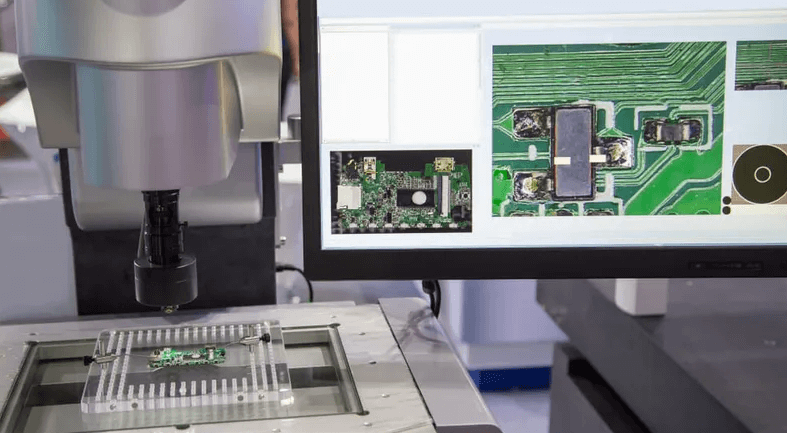
How do we define AOI? Automated optical inspection is the visual inspection of finished circuit boards using a machine scanner that uses light imaging. It assesses workmanship quality to ensure the PCBs are suitable for purchase and use.
AOI systems typically contain multiple light sources and, sometimes, cameras. The light sources illuminate the PCB from different angles, while the cameras take photos or videos to create a comprehensive image for evaluation.
AOI measurements typically use a machine scanner to automatically scan the device, eliminating the need for visual inspection. Scanners can inspect for defects that could lead to catastrophic failure (such as missing critical components) and can also detect smaller defects that can degrade the quality and performance of a PCB. These minor defects might include issues like slightly misaligned components or solder joints of the wrong size or shape.
AOI is useful at many different stages of production. It is used for bare board inspection, solder paste inspection, and pre- and post-reflow. Each stage can introduce defects into the PCB design, and AOI can catch them before they progress to production.
However, in practice, most AOI is performed in post-production. This is because AOI can simultaneously detect multiple defects using a single system. A comprehensive inspection requires less time than performing inspections after each step in the process. Using AOI as a final inspection can help increase production speeds and improve productivity and meeting deadlines. Furthermore, if AOI detects defects in the late production stage, the defective boards can be returned for rework, while the remaining boards can move forward.
The Role of AOI
AOI plays a vital role in PCB production. It ensures that each board meets the high performance required for complex electrical applications.
When an AOI detects defects on a PCB, it flags the board for repair. This process can occur in several different ways. The AOI’s findings may not meet specific facility requirements, such as requiring all traces on a board to exceed a certain size. In this case, a human operator can review the findings and determine which boards should be returned for further work. Alternatively, the AOI can compare the actual PCB with a computer-aided design (CAD) image of a perfect PCB. The AOI can automatically detect where the actual board deviates from the ideal design and flag it for rework.
AOI provides the following benefits to PCB production:
Ensuring Quality: AOI allows you to ensure that your PCB products perform as expected. Ensuring product quality can help improve customer satisfaction, enhance your reputation within your business, and reassure you about the value of the service you provide to your customers.
Evaluating Complex Boards: At Millenium Circuits, if one of our boards contains more than 100 components, it will undergo automated AOI. AOI can inspect complex board designs with a level of precision unmatched by the human eye.
Process Improvement: If a defect is caused by a faulty process, immediately identifying it with AOI can help you determine the defect pattern and adjust the process before thousands of boards with the same defect are produced. A recent study published in the International Journal of Engineering and Advanced Technology reported that the cost of finding a fault on a newly assembled board is only ten times higher than catching a defect on a bare board, but finding a fault on a board already in the field is 1,000 times more expensive. Catching errors early minimizes the potential for future rework and makes your production operations more efficient.
Customizability: AOI is an automated process, but operators can set parameters to tell the scanner what to inspect. If your design specifications change, it’s easy to adjust the settings to detect the defects you need.
How AOI is Reviewed
The following are some of the factors reviewed during AOI:
Soldering Defects
Soldering uses low-melting-point alloys (typically tin and lead) or lead-free alloys to connect the metal components of a PCB. The process is similar to soldering, except that it doesn’t melt the metal components. Soldering defects occur when the connection between two metal components fails to form as expected.
The following are some common soldering defects that AOI can inspect:
1.Open Circuits
Open circuits in PCBs are relatively common defects and are problematic because an incomplete circuit prevents current from flowing. When the circuit is open, the board will not function properly.
Open circuits can occur due to improperly formed vias and traces, or due to soldering that is not done to the target. Visual inspection or X-ray imaging can sometimes detect obvious breaks, but AOI can identify even minor ones and flag them for return to properly close the circuit.
2.Solder Bridges or Shorts
Solder bridges occur when solder connects two components on a PCB that should not be electrically connected. These bridges form when too much solder is used during board production or when solder seeps into areas of the board that are intended to remain solder-free.
Solder bridges often occur when solder is not separated from leads before solidifying. Leads are metal pads designed to connect two locations on the board. Solder may not separate because the leads are too large, too much solder is holding them to the board, or the board pitch is very shallow.
Solder bridges are problematic because they disrupt the intended flow of current through the board. They can cause shorts or burn critical components or traces on the board. They are also notoriously difficult to detect with the naked eye—even tiny solder leaks can lead to the formation of solder bridges. Fortunately, AOI scanning can detect even small solder bridges and send the defective board back for repair.
3.Insufficient Solder
Insufficient solder joints occur when too little solder is used during the production process to connect different components on the board. Sometimes, the solder fails to fully connect the components—this condition is called solder funneling.
When insufficiently soldered components are connected erratically, they may not form a stable electrical connection, and the board will perform poorly. Moreover, if the amount of solder is so fine that it can’t hold it to the board, the board will end up with missing parts, which can potentially lead to catastrophic failure. AOI can scan and note the amount of solder on each component or compare the board to a corrected image to determine if the board needs to be re-soldered.
4.Excess Solder
Excess solder occurs when the opposite occurs—the production process applies too much solder to the board. This sometimes happens because a solder nozzle that’s too wide is used, or because the solder tip is over-applied.
Excess solder can cause a number of problems, including deformities such as solder bridges. When the production process applies too much solder to the pins on the board, it can also create a large, round solder ball, making it difficult to determine whether the pin is adequately wetted and adhered to the board.
Solder balls are relatively easy to detect due to their size, but an inspector might miss one after reviewing dozens of nearly identical boards. A good AOI scanner can easily detect excess solder and send the board back for rework with a solder sucker or solder wick.
Component Defects
Component defects refer to failures in small, functional components connected to the board. The following are some common component defects on PCBs:
- Lifted Leads
Lifted leads occur when one of the tiny metal pads on a PCB fails to adhere properly. Sometimes, lifted leads can occur due to overheating or excessive handling during production, or due to board warping. In other cases, it can cause leads to be too long and lift when they come into contact with solder.
Lifted leads are unstable and therefore problematic. The pads on the board allow the pins to connect to the copper pad below, but if the leads are lifted, the pins won’t make a proper connection. This lost connection can lead to component failure and compromise the board’s performance.
2.Missing Components
PCBs can be missing components for a variety of reasons. Inadequate soldering can cause parts to be missing, or the production process may skip necessary parts.
Missing components is a serious defect on a PCB—it can lead to catastrophic failure. Missing parts may be noticeable to the human eye, but because they are an inevitable failure, having a reliable AOI scanner is crucial to catching PCBs with missing parts before they reach customers.
3.Misplaced or Dislocated Components
Misplaced or dislocated components can occur when parts are incorrectly placed during production or shifted after placement. During reflow soldering, component movement is common because parts easily move above the molten solder—the surface tension of the solder means components slide easily.
If components are misaligned or improperly placed, the PCB may still function, but performance may be slow. Or it may not perform at all. Alignment errors may be too small to be seen with the naked eye, so having a reliable AOI scanner is crucial for catching these defects.
How does AOI compare to other inspection methods?
AOI offers many advantages over other processes for detecting faults in PCBs. Here’s a breakdown of how AOI stacks up against other inspection methods:
4.Automated X-ray Inspection (AXI)
AXI uses X-rays instead of light imaging to inspect PCBs. Companies often use AXI to evaluate particularly complex or densely constructed boards. This is because X-rays travel through materials to image them. Because the light used for AOI reflects off surfaces, one component may block another. However, X-rays pass through different layers of material, accurately imaging all of them.
AXI is a complex and emerging technology, and its main drawback is its high cost. Because AXI is so expensive, it’s generally not worth using unless the board is particularly complex or highly clustered.
2.Automated Laser Test (ALT) Measurement
ALT measurement uses a laser instead of traditional optical imaging to scan and measure the PCB. As light from the laser reflects off PCB components, the ALT system uses the laser’s position to precisely locate the position and height of different components and evaluate their reflectivity. Like AOI, the ALT system can compare empirical measurements to a schematic or set of specifications to detect any defects.
ALT measurement is particularly useful for assessing the placement and amount of solder paste, although interference can sometimes make the measurement inaccurate.
3.In-Circuit Test (ICT)
In-circuit test uses an electrical probe to evaluate how the assembled PCB will function. It uses electrical current to check that each component is in place and functioning properly. It tests for shorts and opens and assesses basic electrical qualities such as capacitance and resistance.
Because it uses electrical current rather than imaging, ICT tends to provide more limited solder information than AOI. It can assess the quality of electrical components and provide information on solder defects affecting the circuit, but it cannot provide detailed information about insufficient or excessive solder.
AOI is generally more reliable than in-circuit testing, especially for the smaller PCBs being developed today.
4.Manual Visual Inspection (MVI)
Most PCB companies prefer AOI to manual visual inspection because AOI doesn’t require contact with the boards. Human inspectors must handle the boards, and handling can introduce defects to an otherwise perfect board. AOI can scan PCBs without disturbing their delicate components and preserving their structural integrity.
AOI is also more reliable than human visual inspection. A human can easily miss a small defect on a PCB. But AOI can catch even the tiniest errors. Its unwavering sensitivity allows it to scan boards in far finer detail than the human eye allows, and it remains reliable throughout all stages of the production process.


