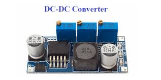
What is DC-DC? How to design PCB for DC-DC?
DC-DC is a device that converts electric energy of one voltage value into electric energy of another voltage value in a DC circuit. DC-DC power modules are widely used in various fields.
1.DC-DC
DC-DC is a device that converts electric energy of one voltage value into electric energy of another voltage value in a DC circuit.
It uses microelectronics technology to assemble small surface-mounted integrated circuits and microelectronic components into one.
DC-DC is a newly developed miniaturized power switch module.
It uses microelectronics technology to assemble small surface-mounted integrated circuits and microelectronic components into one. The use of DC-DC power modules is conducive to simplifying the design of power circuits, shortening the development cycle, achieving optimal indicators, etc., and can be widely used in various digital instruments and intelligent instruments.
DC-DC power modules are widely used in power electronics, military industry, scientific research, industrial control equipment, communication equipment, instrumentation, switching equipment, access equipment, mobile communications, routers and other communication fields and industrial control, automotive electronics, aerospace and other fields.
Since the use of modules to form a power system has the characteristics of short design cycle, high reliability, and easy system upgrade, the application of power modules is becoming more and more extensive.
Especially in recent years, due to the rapid development of data services and the continuous promotion of distributed power supply systems, the growth rate of power modules has exceeded that of primary power supplies. With the extensive use of semiconductor processes, packaging technologies and high-frequency soft switches, the power density of power modules is getting higher and higher, the conversion efficiency is getting higher and higher, and the application is getting simpler and simpler.
2.PCB design of DC-DC
The circuit of DC-DC is much more complicated than that of LDO, the noise is also greater, and the layout and layout requirements are higher. The quality of the layout directly affects the performance of DC-DC, so it is very important to understand the layout of DC-DC.
- Bad layout
EMI, the SW pin of DC-DC will have a higher dv/dt, and a higher dv/dt will cause a larger EMI interference;
Ground noise, poor ground routing will generate a larger switching noise on the ground, and these noises will affect other parts of the circuit;
Voltage drop occurs on the wiring, and if the routing is too long, it will cause a voltage drop on the routing, which will reduce the efficiency of the entire DC-DC;
- General principles
The switching high current loop should be as short as possible;
The signal ground and high current ground (power ground) should be routed separately and connected at a single point at the chip GND;
① Switching loop is short
The red LOOP1 in the figure below is the current flow direction when the DC-DC high-side tube is turned on and the low-side tube is turned off; the green LOOP2 is the current flow direction when the high-side tube is turned off and the low-side tube is turned on;
In order to make these two loops as small as possible and introduce less interference, the following principles need to be followed:
The inductor should be as close to the SW pin as possible;
The input capacitor should be as close to the VIN pin as possible;
The ground of the input and output capacitors should be as close to the PGND pin as possible;
Use copper plating to route;
Why do this?
If the routing is too thin and too long, the impedance will increase, and a large current will generate a relatively high ripple voltage on this large impedance;
If the routing is too thin and too long, the parasitic inductance will increase, and the switching noise will be coupled to this inductance, affecting the stability of the DC-DC and causing EMI problems;
Parasitic capacitance and impedance will increase switching loss and conduction loss, affecting DC-DC efficiency;
② Single-point grounding
Single-point grounding refers to single-point grounding of the signal ground and the power ground. There will be relatively large switching noise on the power ground, so it is necessary to try to avoid interference with sensitive small signals, such as the FB feedback pin.
Large current ground: L, Cin, Cout, Cboot are connected to the large current ground network;
Small current ground: Css, Rfb1, Rfb2 are connected to the signal ground network separately;
3.Example
The following is a layout of a typical DC-DC BUCK circuit. SPEC gives the following points:
The switch loop formed by the input capacitor, high-side MOS tube, and freewheeling diode is as small and short as possible;
The input capacitor is as close to the Vin Pin as possible;
Ensure that all feedback connections are short and direct, and the feedback resistor and compensation components are as close to the chip as possible;
SW is away from sensitive signals such as FB;
Connect VIN, SW, and especially GND to a large copper area to cool the chip and improve thermal performance and long-term reliability;
4.Summary
The layout of the DC-DC circuit is crucial and directly affects the working stability and performance of the DC-DC. Generally, the SPEC of the DC-DC chip will give layout guidance, which can be used as a reference for design. For power components, capacitors and resistors, you can go to Weiyang Mall, which is an original agent. It is really great.