What is Fanout PCB? Requirements for PCB Fanout in PCB Design
Introduction to Fanout in PCB Design
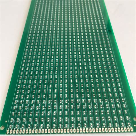
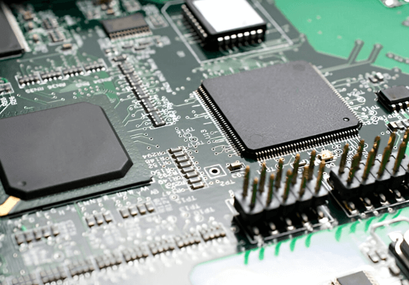
Printed Circuit Board (PCB) design has become increasingly complex with the advancement of electronic technologies, particularly with the proliferation of high-density interconnect (HDI) designs and ball grid array (BGA) components. One critical aspect of modern PCB layout that ensures signal integrity and manufacturability is proper fanout technique. Fanout, often referred to as “fanout PCB” or “PCB fanout,” represents the transitional routing strategy that connects dense component pads (typically on BGAs or fine-pitch components) to wider traces that can be routed across the PCB.
This article will explore the concept of fanout in PCB design, its importance, and the key requirements that designers must consider when implementing fanout strategies. We’ll examine the technical considerations, design rules, and best practices that ensure optimal performance while maintaining manufacturability.
Understanding Fanout PCB
Definition of Fanout
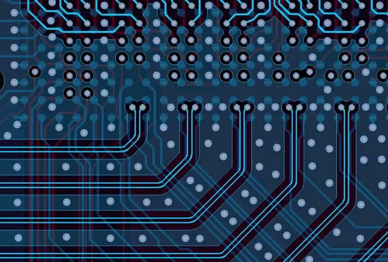
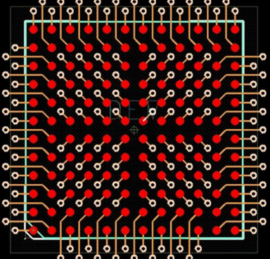
Fanout in PCB design refers to the pattern of traces that “fan out” from densely packed component pins (like those on a BGA package) to less dense areas of the board where routing becomes more manageable. It serves as the bridge between the tight spacing of modern component packages and the wider spacing needed for conventional PCB routing.
The fanout process typically involves:
- Breaking out connections from tight-pitch components
- Transitioning to appropriate trace widths
- Connecting to vias that route signals to other layers
- Spreading out connections to allow proper routing space
Importance of Proper Fanout
Effective fanout is crucial for several reasons:
- Signal Integrity: Proper fanout minimizes crosstalk, impedance mismatches, and signal reflections.
- Manufacturability: Adequate fanout ensures the design can be reliably produced with standard PCB fabrication processes.
- Routing Completion: Good fanout strategies enable 100% routability of complex designs.
- Thermal Management: Appropriate fanout aids in heat dissipation for high-power components.
- Testability: Well-planned fanout allows for proper test point access during manufacturing testing.
Types of Fanout Strategies
Standard Fanout
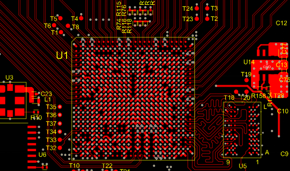
The most common fanout approach for BGA components where:
- Each ball gets its own via
- Vias are placed diagonally between balls
- Routing escapes in perpendicular directions
Staggered Fanout
Used for very dense packages where:
- Vias are offset to maximize space utilization
- Allows for tighter pitch components
- Requires careful planning to avoid conflicts
Microvia Fanout
Essential for HDI designs featuring:
- Laser-drilled microvias (usually 0.1mm or smaller)
- Stacked or staggered via configurations
- Typically used with via-in-pad technology
Partial Fanout
Applied when:
- Not all pins require fanout
- Some signals can be routed on the same layer
- Used to reduce via count and layer count
Key Requirements for PCB Fanout
1. Via Selection and Placement
Via Type Selection:
- Through-hole vias for standard designs
- Blind/buried vias for complex multilayer boards
- Microvias for HDI designs (laser-drilled)
Via Placement Rules:
- Maintain minimum via-to-via spacing (typically 8-10 mil)
- Follow component manufacturer’s recommended via patterns
- Avoid placing vias directly under component bodies when possible
- Consider via tenting (covering with solder mask) for protection
2. Trace Width and Spacing
Width Considerations:
- Match trace width to current requirements
- Maintain consistent impedance for high-speed signals
- Transition gradually from pad to trace width
Spacing Requirements:
- Follow design rules for minimum clearance
- Increase spacing for high-voltage signals
- Maintain uniform spacing where possible
3. Layer Transition Strategy
Multilayer Considerations:
- Plan layer transitions early in the design process
- Minimize the number of layer changes for critical signals
- Use ground vias adjacent to signal vias for return path continuity
Via Spanning:
- Limit the number of layers a via traverses
- Use blind/buried vias to reduce stub effects
- Consider backdrilling for critical high-speed signals
4. Signal Integrity Requirements
Impedance Control:
- Maintain consistent impedance through fanout region
- Account for via stub effects
- Use appropriate dielectric materials
Crosstalk Mitigation:
- Provide adequate spacing between signal traces
- Use ground vias as shielding between sensitive signals
- Avoid parallel routing of noisy and sensitive signals
5. Power Delivery Considerations
Power Pin Fanout:
- Use multiple vias for high-current pins
- Implement solid power planes where possible
- Consider via stitching for improved current capacity
Decoupling Placement:
- Position decoupling capacitors close to power pins
- Minimize loop area between capacitor and IC
- Use appropriate via connections for capacitors
6. Thermal Management
Heat Dissipation:
- Use thermal vias under hot components
- Consider via fill materials (copper, silver, or conductive epoxy)
- Balance thermal and electrical requirements
CTE Matching:
- Account for coefficient of thermal expansion differences
- Use appropriate via plating thickness
- Consider via fill for improved reliability
7. Manufacturability Requirements
Fabrication Constraints:
- Adhere to manufacturer’s capabilities for via size and spacing
- Consider aspect ratio limitations (via depth to diameter)
- Account for plating requirements
Assembly Considerations:
- Avoid via-in-pad unless properly filled and planarized
- Provide adequate spacing for solder mask between vias
- Consider solder wicking prevention techniques
Advanced Fanout Techniques
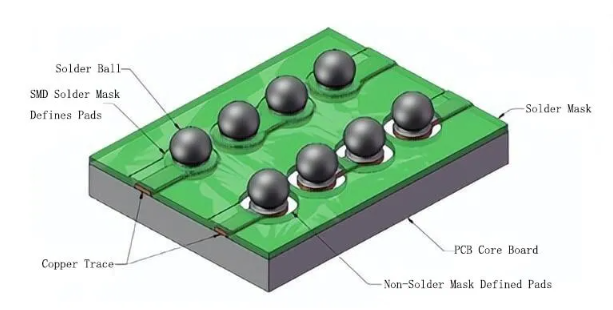
Via-in-Pad Technology
Benefits:
- Saves board space
- Improves signal integrity for high-frequency designs
- Allows for denser component placement
Requirements:
- Requires precise via filling and planarization
- Adds to fabrication cost
- Needs careful thermal management
Any-layer HDI Fanout
Features:
- Enables fanout on any layer combination
- Uses laser-drilled microvias
- Allows for extremely dense designs
Considerations:
- Significant cost increase
- Requires advanced design tools
- Demands close collaboration with fabricator
Backdrilling for High-speed Signals
Purpose:
- Removes unused via stubs
- Improves signal integrity at high frequencies
- Reduces reflections and attenuation
Implementation:
- Requires additional fabrication step
- Needs careful depth control
- Adds to board cost
Design Tools and Automation
Modern PCB design software offers various tools to assist with fanout:
- Automated Fanout Generators: Many ECAD tools provide automated BGA fanout capabilities that can be customized with design rules.
- Design Rule Checking (DRC): Automated verification of fanout against manufacturing constraints.
- Constraint Managers: Allow setting up complex rules for different signal types.
- 3D Visualization: Helps identify potential conflicts in complex fanout scenarios.
While automation can help, experienced designer oversight remains crucial for optimal results.
Common Fanout Mistakes to Avoid
- Insufficient Via Clearance: Causing manufacturing difficulties or reliability issues.
- Improper Via Size Selection: Too small vias may not plate properly; too large waste space.
- Ignoring Return Paths: Especially important for high-speed signals.
- Overlooking Thermal Considerations: Leading to potential reliability problems.
- Inconsistent Impedance: Causing signal integrity issues.
- Poor Layer Transition Planning: Resulting in unnecessary complexity.
- Neglecting Test Access: Making board testing and debugging difficult.
Industry Standards and Guidelines
Several standards inform PCB fanout practices:
- IPC-7351: Generic requirements for surface mount design, including land pattern and fanout considerations.
- IPC-2221/2222: Generic standards for PCB design covering via and routing requirements.
- IPC-6012: Qualification and performance specification for rigid PCBs.
- JEDEC Standards: Particularly for BGA and other package-specific requirements.
- IEEE Standards: For high-speed design considerations.
Designers should consult the relevant standards for their specific application and industry requirements.
Future Trends in PCB Fanout
- Smaller Via Sizes: Continued reduction to support higher density packages.
- Advanced Materials: New dielectric materials enabling better high-frequency performance.
- Embedded Components: Reducing the need for some fanout requirements.
- 3D Packaging: Changing traditional fanout approaches.
- AI-assisted Design: More intelligent fanout automation tools.
Conclusion
PCB fanout is a critical aspect of modern electronic design that bridges the gap between increasingly dense component packages and practical routing requirements. Proper fanout implementation requires careful consideration of numerous factors including signal integrity, power delivery, thermal management, and manufacturability.
By understanding the various fanout strategies and adhering to established design requirements, PCB designers can create robust, high-performance boards that meet both technical and production needs. As component densities continue to increase and signal speeds rise, the importance of proper fanout techniques will only grow more critical.
The most successful designs come from balancing all these requirements while working closely with fabrication partners to ensure designs are both optimal and manufacturable. With careful planning and attention to detail, designers can implement fanout strategies that support today’s complex electronic systems while being prepared for tomorrow’s challenges.