What is pcb in electronics
Introduction To what is pcb in electronics
Printed Circuit Boards (PCBs) are fundamental components in the realm of modern electronics, serving as the backbone upon which virtually all electronic devices are built.
These intricate boards are designed to mechanically support and electrically connect electronic components using conductive pathways, tracks, or signal traces etched from copper sheets laminated onto a non-conductive substrate.
The advent of PCBs has revolutionized the electronics industry, enabling the miniaturization and increased functionality of electronic devices.
To understand the significance of PCBs, it is essential to delve into their structure and function.
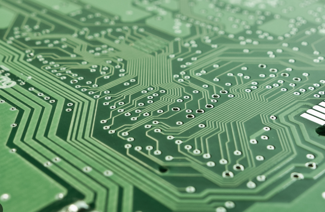
A typical PCB consists of multiple layers, including a substrate, copper layers, solder mask, and silkscreen. The substrate, often made of fiberglass-reinforced epoxy resin, provides the board with its rigidity and insulating properties. Copper layers are then added to create the necessary electrical pathways. The solder mask, a protective layer, prevents short circuits and corrosion, while the silkscreen layer is used to print labels and symbols on the board for easier assembly and troubleshooting.
The process of manufacturing a PCB involves several meticulous steps, beginning with the design phase.
Engineers use specialized software to create a schematic diagram, which is then translated into a layout that specifies the exact placement of components and routing of electrical connections. This layout is used to produce a photomask, which guides the etching process. During etching, unwanted copper is removed, leaving behind the desired circuit pattern. Subsequent steps include drilling holes for component leads, applying the solder mask, and printing the silkscreen. Finally, the board undergoes a series of inspections and tests to ensure its functionality and reliability.
PCBs come in various types, each tailored to specific applications.
Single-sided PCBs, with components and traces on one side only, are the simplest and most cost-effective. Double-sided PCBs, featuring traces on both sides, offer greater complexity and are suitable for more advanced circuits. Multi-layer PCBs, which consist of multiple layers of substrate and circuitry stacked together, provide even higher levels of complexity and are used in sophisticated devices such as smartphones and computers. Flexible PCBs, made from flexible materials, can be bent and folded, making them ideal for applications where space constraints are a concern.
The advantages of using PCBs in electronic devices are manifold.
They offer a compact and organized way to connect components, reducing the likelihood of wiring errors and improving overall reliability. PCBs also facilitate mass production, as they can be manufactured in large quantities with consistent quality. Additionally, the use of PCBs enhances the performance of electronic devices by minimizing electrical noise and interference, thanks to the precise control over the layout of traces and components.
In conclusion, Printed Circuit Boards are indispensable to the modern electronics industry, providing the essential framework for the assembly and operation of electronic devices. Their intricate design and manufacturing processes enable the creation of compact, reliable, and high-performance electronics that have become integral to our daily lives. As technology continues to advance, the role of PCBs will undoubtedly remain pivotal, driving innovation and shaping the future of electronics.
How PCBs Revolutionized Electronic Circuit Design
Printed Circuit Boards (PCBs) have fundamentally transformed the landscape of electronic circuit design, ushering in a new era of efficiency, reliability, and miniaturization. Before the advent of PCBs, electronic circuits were constructed using point-to-point wiring, a labor-intensive and error-prone process that limited the complexity and scalability of electronic devices. The introduction of PCBs marked a significant departure from these rudimentary methods, offering a more streamlined and robust approach to circuit assembly.
At the core of a PCB is a non-conductive substrate, typically made from materials such as fiberglass or composite epoxy.
This substrate provides a stable foundation upon which conductive pathways, or traces, are etched. These traces are usually composed of copper, chosen for its excellent electrical conductivity and ease of etching. The design of these pathways is meticulously planned using computer-aided design (CAD) software, ensuring that electrical signals can travel efficiently between components with minimal interference or loss.
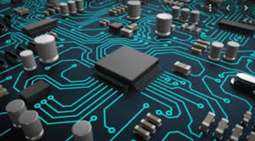
One of the most profound impacts of PCBs on electronic circuit design is the ability to integrate a multitude of components into a compact and organized layout.
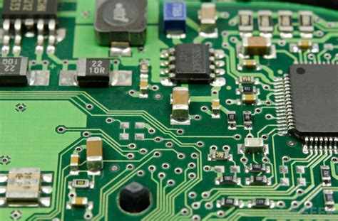
Surface-mount technology (SMT) and through-hole technology are two primary methods used to attach components to a PCB. SMT allows components to be mounted directly onto the surface of the board, significantly reducing the size and weight of the final product. Through-hole technology, on the other hand, involves inserting component leads into pre-drilled holes and soldering them in place, providing a more secure mechanical bond. The combination of these techniques enables the creation of highly complex circuits that are both reliable and space-efficient.
Moreover, PCBs have enhanced the reliability and durability of electronic devices.
The fixed layout of traces and components minimizes the risk of loose connections and short circuits, common issues in point-to-point wiring. Additionally, the use of solder masks and protective coatings shields the board from environmental factors such as moisture and dust, further extending the lifespan of the device. This increased reliability is particularly crucial in applications where failure is not an option, such as in medical devices, aerospace, and automotive systems.
The standardization brought about by PCBs has also facilitated mass production and scalability in the electronics industry.
Once a PCB design is finalized, it can be reproduced with high precision and consistency, ensuring that each unit performs identically. This repeatability is essential for manufacturers aiming to produce large quantities of electronic devices without compromising on quality. Furthermore, automated assembly processes, such as pick-and-place machines and reflow soldering, have significantly reduced production times and costs, making advanced electronics more accessible to consumers.
In addition to these practical advantages, PCBs have also driven innovation in electronic design.
The ability to create multi-layer boards, where multiple layers of traces are stacked and interconnected through vias, has opened up new possibilities for circuit complexity and functionality. This has enabled the development of sophisticated technologies such as smartphones, computers, and advanced communication systems, which rely on densely packed and highly integrated circuits.
In conclusion, the advent of PCBs has revolutionized electronic circuit design by providing a reliable, efficient, and scalable method for assembling complex circuits. The transition from point-to-point wiring to PCB-based designs has not only improved the performance and durability of electronic devices but has also paved the way for rapid advancements in technology. As the electronics industry continues to evolve, PCBs will undoubtedly remain a cornerstone of innovation and progress.
The Manufacturing Process Of PCBs: From Design To Production
The manufacturing process of Printed Circuit Boards (PCBs) is a meticulous and intricate procedure that transforms a conceptual design into a functional electronic component. This journey begins with the design phase, where engineers utilize specialized software to create a detailed schematic of the PCB.
These schematics outline the electrical pathways and component placements, ensuring that the final product will operate as intended. Once the design is finalized, it is converted into a format known as Gerber files, which serve as the blueprint for the subsequent manufacturing stages.
Transitioning from design to production, the first step involves the creation of the PCB substrate, typically made from fiberglass-reinforced epoxy resin, known as FR4.
This substrate provides the structural foundation for the PCB. A thin layer of copper is then laminated onto both sides of the substrate, forming the basis for the conductive pathways. The next phase, known as photoresist application, involves coating the copper-clad substrate with a light-sensitive material. This material will later be used to transfer the circuit design onto the copper layer.
Following the application of the photoresist, the substrate is exposed to ultraviolet (UV) light through a photomask, which contains the circuit pattern.
The UV light hardens the photoresist in the areas exposed through the photomask, while the unexposed areas remain soft and can be washed away. This process effectively transfers the circuit design onto the copper layer. Subsequently, the board undergoes an etching process, where a chemical solution removes the unprotected copper, leaving behind only the desired circuit pathways.
After etching, the remaining photoresist is stripped away, revealing the copper traces that form the circuit.
The next step involves drilling holes for component leads and vias, which are essential for establishing electrical connections between different layers of the PCB. Precision drilling machines equipped with tiny drill bits are used to create these holes with high accuracy. Once the drilling is complete, the holes are plated with copper to ensure electrical conductivity.
The PCB then undergoes a process called solder mask application, where a protective layer is applied to insulate the copper traces and prevent short circuits.
The solder mask also provides a surface for soldering components onto the board. Following this, a silkscreen layer is added, which prints labels and markings on the PCB to assist in component placement and identification.
As the PCB nears completion, it undergoes a series of rigorous inspections and tests to ensure quality and functionality. Automated optical inspection (AOI) systems are employed to detect any defects or inconsistencies in the circuit pattern. Additionally, electrical tests are conducted to verify the continuity and integrity of the circuits. Any identified issues are addressed before proceeding to the final stages.
The final step in the manufacturing process is the assembly of electronic components onto the PCB.
This involves placing and soldering components such as resistors, capacitors, and integrated circuits onto the board. Surface-mount technology (SMT) and through-hole technology are commonly used methods for component placement. Once all components are securely attached, the assembled PCB undergoes a final inspection and testing phase to ensure it meets all specifications and performance criteria.
In conclusion, the manufacturing process of PCBs is a complex and precise endeavor that requires careful planning, advanced technology, and stringent quality control measures. From the initial design to the final production, each step is crucial in creating a reliable and functional electronic component that forms the backbone of modern electronic devices.
Common Types Of PCBs And Their Applications In Electronics
Printed Circuit Boards (PCBs) are fundamental components in modern electronics, serving as the backbone for virtually all electronic devices. They provide the physical platform upon which electronic components are mounted and interconnected. Understanding the common types of PCBs and their applications is crucial for anyone involved in electronics design and manufacturing.
Single-sided PCBs are the simplest type, featuring a single layer of conductive material, typically copper, on one side of a non-conductive substrate.
These boards are cost-effective and easy to manufacture, making them ideal for low-density designs and consumer electronics such as calculators, remote controls, and simple sensors. Despite their simplicity, single-sided PCBs are limited in their ability to support complex circuits due to the restricted space for routing traces.
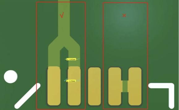
Double-sided PCBs, on the other hand, have conductive layers on both sides of the substrate.
This configuration allows for more complex circuitry and higher component density. Vias, or small holes plated with conductive material, are used to connect traces on both sides of the board. Double-sided PCBs are commonly found in applications such as power supplies, amplifiers, and more sophisticated consumer electronics. Their increased complexity and capability make them a versatile choice for a wide range of electronic devices.
Moving to more advanced designs, multi-layer PCBs consist of multiple layers of conductive material separated by insulating layers.
These boards can have anywhere from three to over a dozen layers, allowing for extremely complex and high-density circuit designs. Multi-layer PCBs are essential in applications where space is at a premium and performance is critical, such as in smartphones, computers, and medical devices. The additional layers provide more routing options and can help reduce electromagnetic interference, improving the overall performance of the device.
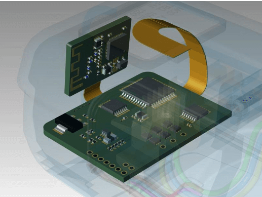
Flexible PCBs, or flex PCBs, are designed to bend and flex, making them suitable for applications where the board needs to conform to a specific shape or fit into a tight space.
These boards are made from flexible materials such as polyimide, which can withstand bending and twisting without breaking. Flex PCBs are commonly used in wearable electronics, flexible displays, and medical devices where traditional rigid PCBs would be impractical. Their ability to flex and fold opens up new possibilities in electronic design, enabling more innovative and compact devices.
Rigid-flex PCBs combine the benefits of both rigid and flexible PCBs.
These boards consist of multiple layers of flexible circuit substrates attached to one or more rigid boards. This hybrid design allows for greater mechanical stability and reliability while still offering the flexibility needed for complex applications. Rigid-flex PCBs are often used in aerospace, military, and medical applications where reliability and performance are paramount. They provide a robust solution for devices that require both rigid and flexible elements, such as in advanced communication systems and implantable medical devices.
In conclusion, the various types of PCBs each offer unique advantages and are suited to different applications in the electronics industry. Single-sided and double-sided PCBs are ideal for simpler, cost-effective designs, while multi-layer PCBs cater to high-density, high-performance applications. Flexible and rigid-flex PCBs provide the versatility needed for innovative and compact designs. Understanding these different types of PCBs and their applications is essential for anyone involved in the design and manufacturing of electronic devices, as it allows for the selection of the most appropriate PCB type to meet specific design requirements and performance criteria.