What is pcb manufacturing
Introduction To PCB Manufacturing: Understanding The Basics
Printed Circuit Board (PCB) manufacturing is a complex and intricate process that forms the backbone of modern electronic devices. Understanding the basics of PCB manufacturing is essential for anyone involved in electronics, whether as a hobbyist, engineer, or industry professional. The journey of a PCB from concept to finished product involves several critical steps, each requiring precision and expertise.
Initially, the process begins with the design phase, where engineers use specialized software to create a schematic diagram of the circuit.
This schematic serves as a blueprint, detailing the electrical connections and components required for the PCB. Once the schematic is finalized, it is converted into a layout, which specifies the physical arrangement of components and the routing of electrical traces on the board. This layout is then used to generate Gerber files, which are the standard format for PCB manufacturing.
Following the design phase, the next step is the fabrication of the PCB.
This involves creating the physical board from a substrate material, typically fiberglass-reinforced epoxy laminate, known as FR4. The substrate is coated with a layer of copper, which will form the conductive pathways of the circuit. The copper layer is then covered with a photosensitive film, and the Gerber files are used to create a photomask. This photomask is used to expose the film to ultraviolet light, hardening the areas that will remain as conductive traces.
After exposure, the board undergoes a chemical etching process to remove the unexposed copper, leaving behind the desired circuit pattern.
The next step is drilling, where precise holes are made for component leads and vias, which are used to connect different layers of the PCB. These holes are then plated with copper to ensure electrical continuity.
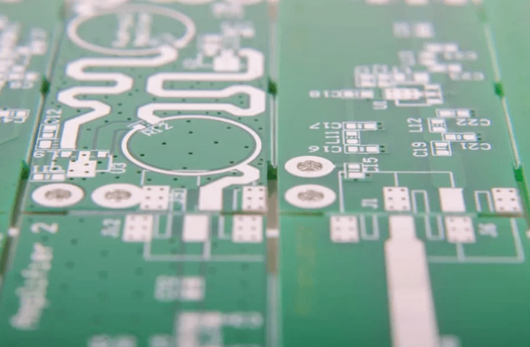
Subsequently, the board is cleaned and coated with a solder mask, which is a protective layer that prevents solder bridges and short circuits during component assembly. The solder mask is typically green, although other colors are also used. Silkscreen printing is then applied to add labels and markings, aiding in component placement and identification.
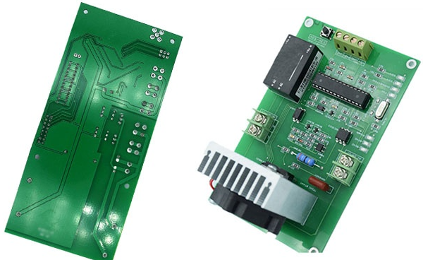
The final stage of PCB manufacturing is assembly, where components are mounted onto the board.
This can be done using either through-hole technology, where component leads are inserted into drilled holes and soldered, or surface-mount technology (SMT), where components are placed directly onto the surface of the board and soldered using reflow soldering. SMT is more common in modern electronics due to its efficiency and ability to accommodate smaller components.
Quality control is a crucial aspect of PCB manufacturing, ensuring that each board meets the required specifications and functions correctly. This involves visual inspections, automated optical inspections (AOI), and electrical testing to detect any defects or issues. Once the boards pass these tests, they are ready for integration into electronic devices.
In conclusion, PCB manufacturing is a multifaceted process that requires careful planning, precise execution, and rigorous quality control. From the initial design to the final assembly, each step is vital in producing reliable and high-performance PCBs. Understanding these basics provides a foundation for appreciating the complexity and importance of PCBs in the world of electronics.
Key Steps In The PCB Manufacturing Process
Printed Circuit Board (PCB) manufacturing is a complex process that involves several critical steps to ensure the final product meets the required specifications and quality standards. The journey begins with the design phase, where engineers use specialized software to create a detailed blueprint of the PCB. This design includes the layout of the electrical components and the pathways that will connect them. Once the design is finalized, it is converted into a format that can be used for manufacturing, typically Gerber files.
Following the design phase, the next step is the creation of the PCB substrate, which serves as the foundation of the board.
The substrate is usually made from a non-conductive material such as fiberglass or epoxy resin. A thin layer of copper is then laminated onto the substrate to form the conductive pathways. This copper layer is essential for the subsequent steps, as it will be etched to create the circuit patterns.
The process of transferring the circuit design onto the copper layer is known as photolithography.
During this step, a photosensitive film is applied to the copper-clad substrate. The film is then exposed to ultraviolet light through a mask that contains the circuit design. The areas of the film exposed to the light harden, while the unexposed areas remain soft and can be washed away. This leaves a precise pattern of the circuit design on the copper layer.
Etching is the next crucial step in PCB manufacturing.
In this process, the board is exposed to a chemical solution that removes the unprotected copper, leaving behind only the desired circuit pathways. The etching process must be carefully controlled to ensure that the pathways are not over-etched or under-etched, as this can affect the performance of the final PCB.
After etching, the next step is drilling.
Holes are drilled into the PCB to accommodate the leads of electronic components and to create vias, which are pathways that allow electrical connections between different layers of the board. The drilling process requires high precision, as the holes must be accurately positioned and sized to match the design specifications.
Once the holes are drilled, the PCB undergoes a plating process.
This involves depositing a thin layer of conductive material, usually copper, onto the walls of the drilled holes. This step is essential for creating reliable electrical connections between the different layers of the PCB.
Following plating, the PCB is subjected to a solder mask application.
The solder mask is a protective layer that covers the entire board except for the areas where components will be soldered. This layer helps prevent short circuits and protects the copper pathways from oxidation and other environmental factors.
The final step in the PCB manufacturing process is the application of the silkscreen. This involves printing labels, symbols, and other markings onto the board to assist with component placement and identification during assembly. The silkscreen is typically applied using a specialized printing process that ensures high accuracy and durability.
In conclusion, PCB manufacturing is a multi-step process that requires precision and attention to detail at every stage. From design and substrate preparation to etching, drilling, plating, and final finishing, each step plays a crucial role in producing a high-quality PCB that meets the required specifications. Understanding these key steps provides valuable insight into the complexity and importance of PCB manufacturing in the electronics industry.
Advanced Techniques In Modern PCB Manufacturing
Printed Circuit Board (PCB) manufacturing has evolved significantly over the years, driven by the increasing complexity and miniaturization of electronic devices. Advanced techniques in modern PCB manufacturing have emerged to meet the demands of high-performance, reliable, and compact electronic products. These techniques encompass a range of processes and technologies that enhance the precision, efficiency, and functionality of PCBs.
One of the most notable advancements in PCB manufacturing is the use of High-Density Interconnect (HDI) technology.
HDI PCBs are characterized by their higher wiring density per unit area compared to traditional PCBs. This is achieved through the use of microvias, blind vias, and buried vias, which allow for more interconnections in a smaller space. The implementation of HDI technology enables the production of smaller, lighter, and more powerful electronic devices, making it a critical component in the development of modern smartphones, tablets, and other compact gadgets.
In addition to HDI technology, the adoption of advanced materials has played a crucial role in modern PCB manufacturing.
Traditional PCBs are typically made from FR-4, a composite material composed of woven fiberglass cloth with an epoxy resin binder. However, the increasing demand for high-frequency and high-speed applications has led to the use of advanced materials such as Rogers, Teflon, and ceramic substrates. These materials offer superior electrical properties, thermal stability, and mechanical strength, making them ideal for applications in telecommunications, aerospace, and military industries.
Another significant advancement in PCB manufacturing is the integration of flexible and rigid-flex PCBs.
Flexible PCBs are made from flexible materials such as polyimide, allowing them to bend and fold without breaking. Rigid-flex PCBs combine the benefits of both rigid and flexible PCBs, providing a versatile solution for complex electronic designs. These types of PCBs are particularly useful in applications where space constraints and mechanical stress are critical factors, such as in medical devices, wearable technology, and automotive electronics.
The advent of advanced manufacturing techniques such as laser drilling and direct imaging has also revolutionized PCB production.
Laser drilling allows for the creation of extremely small and precise vias, which are essential for HDI PCBs. Direct imaging, on the other hand, replaces traditional photolithography processes with laser-based imaging, resulting in higher resolution and accuracy. These techniques not only improve the quality and reliability of PCBs but also reduce production time and costs.
Moreover, the implementation of automated optical inspection (AOI) and automated X-ray inspection (AXI) systems has significantly enhanced the quality control process in PCB manufacturing.
AOI systems use high-resolution cameras to inspect PCBs for defects such as misaligned components, soldering issues, and surface irregularities. AXI systems, meanwhile, utilize X-ray technology to detect hidden defects within the PCB layers, such as voids, cracks, and insufficient solder joints. These automated inspection systems ensure that PCBs meet stringent quality standards and reduce the likelihood of failures in the final product.
Furthermore, the rise of Industry 4.0 and the Internet of Things (IoT) has led to the integration of smart manufacturing practices in PCB production.
Smart factories leverage data analytics, machine learning, and real-time monitoring to optimize production processes, improve yield rates, and reduce waste. This digital transformation enables manufacturers to respond quickly to market demands, customize products, and maintain a competitive edge in the industry.
In conclusion, advanced techniques in modern PCB manufacturing have significantly transformed the industry, enabling the production of high-performance, reliable, and compact electronic devices. The adoption of HDI technology, advanced materials, flexible and rigid-flex PCBs, laser drilling, direct imaging, automated inspection systems, and smart manufacturing practices has collectively contributed to the evolution of PCB manufacturing. As technology continues to advance, we can expect further innovations that will continue to push the boundaries of what is possible in the world of electronics.
Common Challenges And Solutions In PCB Manufacturing
Printed Circuit Board (PCB) manufacturing is a complex process that involves several stages, each presenting its own set of challenges. Understanding these challenges and their corresponding solutions is crucial for ensuring the production of high-quality PCBs.
One of the most common challenges in PCB manufacturing is maintaining precision during the etching process.
Etching involves removing unwanted copper from the board to create the desired circuit patterns. However, variations in etching rates can lead to over-etching or under-etching, which can compromise the integrity of the circuit. To mitigate this issue, manufacturers often employ advanced etching techniques and regularly calibrate their equipment to ensure consistent results.
Another significant challenge is the alignment of multi-layer PCBs.
As the demand for more compact and complex electronic devices increases, so does the need for multi-layer PCBs. Aligning these layers accurately is critical to the board’s functionality. Misalignment can result in short circuits or open circuits, rendering the PCB useless. To address this, manufacturers use sophisticated alignment systems and optical inspection tools to ensure that each layer is perfectly aligned before proceeding to the next stage of production.
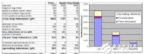
Thermal management is also a critical concern in PCB manufacturing.
As electronic components become more powerful, they generate more heat, which can affect the performance and longevity of the PCB. Effective thermal management involves selecting appropriate materials and designing the PCB layout to facilitate heat dissipation. Techniques such as using thermal vias, heat sinks, and thermal pads are commonly employed to manage heat effectively.
Soldering is another area where challenges frequently arise.
Poor soldering can lead to weak joints, which can cause intermittent connections or complete failure of the PCB. To ensure high-quality soldering, manufacturers use automated soldering machines and conduct rigorous quality control checks. Additionally, the use of lead-free solder, which is more environmentally friendly but has a higher melting point, requires precise temperature control to avoid damaging the components.
Contamination is a pervasive issue that can affect various stages of PCB manufacturing.
Dust, moisture, and other contaminants can lead to defects such as short circuits or corrosion. To combat this, manufacturers implement strict cleanroom protocols and use anti-static materials to minimize contamination. Regular cleaning and maintenance of equipment also play a crucial role in maintaining a contaminant-free environment.
Testing and quality assurance are indispensable in identifying and rectifying defects before the PCBs reach the end-users.
Automated Optical Inspection (AOI) and X-ray inspection are commonly used to detect defects that are not visible to the naked eye. Functional testing, where the PCB is tested under real-world conditions, is also essential to ensure that it meets the required specifications.
Supply chain issues can also pose significant challenges in PCB manufacturing.
Delays in the supply of raw materials or components can disrupt the production schedule, leading to increased costs and delayed deliveries. To mitigate this, manufacturers often establish strong relationships with multiple suppliers and maintain a buffer stock of critical materials.
In conclusion, PCB manufacturing is fraught with challenges that require meticulous attention to detail and advanced technological solutions. From precision in etching and alignment to effective thermal management and rigorous quality control, each stage of the process demands careful consideration. By addressing these challenges proactively, manufacturers can ensure the production of reliable and high-quality PCBs that meet the ever-evolving demands of the electronics industry.