What is PCB Reflow and How to Solve It?
Introduction
Printed Circuit Board (PCB) manufacturing involves multiple complex processes, and reflow soldering is one of the most critical steps in surface-mount technology (SMT). PCB reflow refers to the process of melting solder paste to form reliable electrical connections between surface-mount components and the PCB. However, issues such as poor solder joints, component misalignment, and thermal stress can arise during reflow, leading to defects.
This article explores what PCB reflow is, common problems associated with it, and effective solutions to ensure high-quality solder joints.
1. What is PCB Reflow?
Reflow soldering is a process where solder paste (a mixture of tiny solder particles and flux) is applied to PCB pads, followed by component placement. The PCB then passes through a reflow oven, where controlled heating melts the solder, forming permanent connections.
Stages of Reflow Soldering:
- Preheat Zone – Gradually raises the temperature to activate the flux and remove moisture.
- Soak Zone – Stabilizes temperature to ensure even heat distribution.
- Reflow Zone – Solder paste melts (typically at 217–250°C for lead-free solder).
- Cooling Zone – Solidifies solder joints to ensure mechanical strength.
Common Reflow Defects:
- Cold Solder Joints – Insufficient heat causes weak connections.
- Solder Bridging – Excess solder creates short circuits.
- Tombstoning – One end of a component lifts due to uneven heating.
- Voiding – Gas bubbles trapped in solder joints weaken conductivity.
- Component Misalignment – Improper placement before reflow.

2. Causes of PCB Reflow Issues
Understanding the root causes of reflow defects helps in implementing effective solutions.
A. Temperature Profile Issues
- Incorrect ramp-up rate – Too fast or too slow heating affects flux activation.
- Peak temperature too high/low – Excessive heat damages components, while insufficient heat causes cold joints.
- Uneven heating – Leads to tombstoning or warping.
B. Solder Paste Problems
- Expired or poor-quality solder paste – Reduces wetting ability.
- Incorrect stencil thickness – Too much or too little solder paste application.
C. PCB Design & Manufacturing Flaws
- Poor pad design – Incorrect pad size or spacing causes bridging.
- Insufficient thermal relief – Leads to uneven heating.
- Contaminated surfaces – Oxidation or residues prevent proper solder bonding.
D. Component & Placement Issues
- Mismatched component sizes – Incorrect footprint leads to misalignment.
- Poor pick-and-place accuracy – Misaligned components before reflow.
3. How to Solve PCB Reflow Problems?
A. Optimizing the Reflow Profile
- Use a proper temperature curve – Adjust preheat, soak, reflow, and cooling phases.
- Thermocouple testing – Verify real-time temperature distribution on the PCB.
- Match solder paste specifications – Follow manufacturer-recommended profiles.
B. Improving Solder Paste Quality & Application
- Use fresh solder paste – Store at proper temperature (2–10°C).
- Correct stencil design – Ensure proper thickness (typically 0.1–0.15mm).
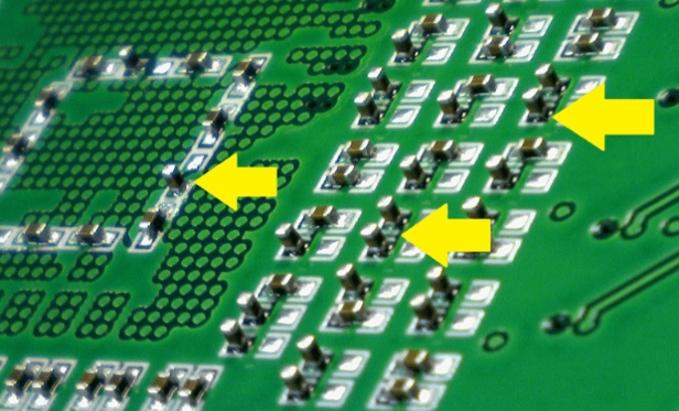
- Inspect paste deposition – Use SPI (Solder Paste Inspection) machines.
C. Enhancing PCB Design & Manufacturing
- Optimize pad geometry – Ensure proper spacing and size.
- Implement thermal balancing – Use copper pours for even heating.
- Clean PCB surfaces – Remove oxidation with proper surface finishes (ENIG, OSP, HASL).
D. Component & Placement Best Practices
- Verify component footprints – Match datasheet specifications.
- Use high-accuracy pick-and-place machines – Minimize misalignment.
- Avoid tombstoning – Ensure symmetrical pad sizes for small components (e.g., resistors, capacitors).
E. Post-Reflow Inspection & Testing
- Automated Optical Inspection (AOI) – Detects solder bridges, misalignment.
- X-ray inspection – Checks for hidden defects like voids.
- Functional testing – Ensures electrical performance.
4. Advanced Solutions for High-Density PCBs
As PCBs become more complex (e.g., HDI, fine-pitch BGAs), reflow challenges increase. Solutions include:
- Nitrogen reflow ovens – Reduce oxidation for better wetting.
- Vacuum reflow – Eliminates voids in high-reliability applications.
- Laser soldering – Precision soldering for sensitive components.
5. Conclusion
PCB reflow is a critical process in SMT assembly, but defects can lead to reliability issues. By optimizing temperature profiles, improving solder paste application, refining PCB design, and using advanced inspection techniques, manufacturers can minimize reflow defects and enhance product quality.
Continuous monitoring, process validation, and adherence to industry standards (IPC-A-610, J-STD-020) ensure consistent and reliable PCB assembly. Implementing these best practices will lead to fewer defects, lower costs, and higher-performing electronic products.