What is portable high frequency pcb
Introduction To Portable High Frequency PCB: Key Features And Benefits
Portable high frequency printed circuit boards (PCBs) represent a significant advancement in the field of electronics, offering a range of features and benefits that cater to the evolving needs of modern technology.
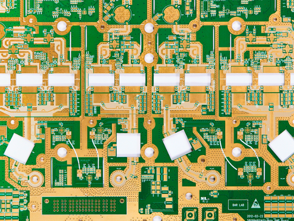
These PCBs are designed to operate at high frequencies, typically above 500 MHz, and are used in applications where signal integrity and performance are critical. The introduction of portable high frequency PCBs has revolutionized various industries, including telecommunications, aerospace, and medical devices, by providing reliable and efficient solutions for high-speed electronic applications.
One of the key features of portable high frequency PCBs is their ability to handle high-speed signals with minimal loss and distortion.
This is achieved through the use of specialized materials and advanced manufacturing techniques that ensure the integrity of the signal is maintained even at high frequencies. Materials such as polytetrafluoroethylene (PTFE) and other low-loss laminates are commonly used in the construction of these PCBs, providing excellent dielectric properties and reducing signal attenuation. Additionally, the precise control of impedance and the use of advanced signal routing techniques further enhance the performance of these PCBs.
Another important feature of portable high frequency PCBs is their compact and lightweight design.
As electronic devices continue to shrink in size, the demand for smaller and more efficient PCBs has increased. Portable high frequency PCBs are designed to meet this demand by offering a high level of functionality in a compact form factor. This is particularly beneficial in applications where space is limited, such as in mobile devices, wearable technology, and compact communication systems. The lightweight nature of these PCBs also makes them ideal for use in aerospace and other industries where weight reduction is a critical factor.
The benefits of portable high frequency PCBs extend beyond their physical characteristics.
One of the most significant advantages is their ability to support high-speed data transmission, which is essential for modern communication systems. With the increasing demand for faster data rates and higher bandwidth, portable high frequency PCBs provide a reliable solution for transmitting large amounts of data quickly and efficiently. This is particularly important in applications such as 5G networks, satellite communications, and high-speed data links, where performance and reliability are paramount.
In addition to their high-speed capabilities, portable high frequency PCBs also offer excellent thermal management properties.
The materials used in these PCBs are designed to dissipate heat effectively, ensuring that the components remain within their optimal operating temperature range. This is crucial in high-frequency applications where excessive heat can lead to signal degradation and component failure. By maintaining proper thermal management, portable high frequency PCBs help to ensure the longevity and reliability of the electronic devices in which they are used.
Furthermore, the versatility of portable high frequency PCBs makes them suitable for a wide range of applications.
From consumer electronics to industrial automation, these PCBs can be customized to meet the specific requirements of different industries. The ability to design and manufacture PCBs with varying levels of complexity and functionality allows for greater flexibility in product development and innovation.
In conclusion, portable high frequency PCBs offer a host of features and benefits that make them an indispensable component in modern electronic systems. Their ability to handle high-speed signals, compact and lightweight design, support for high-speed data transmission, excellent thermal management properties, and versatility make them ideal for a wide range of applications. As technology continues to advance, the demand for portable high frequency PCBs is expected to grow, driving further innovation and development in this critical area of electronics.
Applications Of Portable High Frequency PCB In Modern Electronics
Portable high frequency printed circuit boards (PCBs) have become integral components in the realm of modern electronics, offering a myriad of applications that enhance the functionality and efficiency of various devices. These advanced PCBs are designed to operate at high frequencies, typically above 500 MHz, and are characterized by their ability to handle rapid signal transmission with minimal loss. The applications of portable high frequency PCBs are diverse, spanning across multiple industries and contributing significantly to technological advancements.
One of the primary applications of portable high frequency PCBs is in the telecommunications sector.
With the ever-increasing demand for faster and more reliable communication networks, these PCBs play a crucial role in the development of devices such as smartphones, tablets, and wireless communication systems. The high frequency capabilities of these PCBs enable them to support the high-speed data transmission required for 4G and 5G networks, ensuring seamless connectivity and improved performance. Furthermore, their portability allows for the creation of compact and lightweight devices, which are essential in the modern, mobile-centric world.
In addition to telecommunications, portable high frequency PCBs are extensively used in the aerospace and defense industries.
The stringent requirements for reliability, precision, and performance in these sectors necessitate the use of advanced PCB technology. High frequency PCBs are employed in radar systems, satellite communications, and various avionics applications, where they facilitate the rapid processing and transmission of critical data. Their ability to operate efficiently in harsh environments, coupled with their compact size, makes them ideal for use in military and aerospace equipment.
The medical field also benefits significantly from the applications of portable high frequency PCBs.
Medical devices such as MRI machines, ultrasound equipment, and portable diagnostic tools rely on these PCBs for their high-speed signal processing capabilities. The precision and reliability offered by high frequency PCBs are crucial in medical diagnostics and treatment, where accurate and timely data is paramount. Moreover, the portability of these PCBs enables the development of compact and user-friendly medical devices, which can be easily transported and used in various healthcare settings.
Consumer electronics is another domain where portable high frequency PCBs have made a substantial impact.
From high-definition televisions and gaming consoles to advanced audio systems and wearable technology, these PCBs are at the heart of many modern electronic devices. Their ability to support high-speed data transfer and processing ensures that consumer electronics deliver superior performance and user experience. Additionally, the compact nature of portable high frequency PCBs allows for the design of sleek and lightweight devices, which are highly sought after in the consumer market.
The automotive industry is also witnessing a growing adoption of portable high frequency PCBs.
With the advent of advanced driver-assistance systems (ADAS), electric vehicles (EVs), and autonomous driving technology, the need for high-speed data processing and communication within vehicles has become paramount. High frequency PCBs are used in various automotive applications, including radar and lidar systems, infotainment systems, and vehicle-to-everything (V2X) communication. Their ability to handle high-frequency signals ensures the efficient operation of these advanced automotive technologies, contributing to safer and more connected driving experiences.
In conclusion, the applications of portable high frequency PCBs in modern electronics are vast and varied, spanning across telecommunications, aerospace, defense, medical, consumer electronics, and automotive industries.
Their high-speed signal processing capabilities, reliability, and compact size make them indispensable in the development of advanced electronic devices. As technology continues to evolve, the role of portable high frequency PCBs in driving innovation and enhancing the performance of modern electronics will undoubtedly become even more significant.
Design Considerations For Portable High Frequency PCB
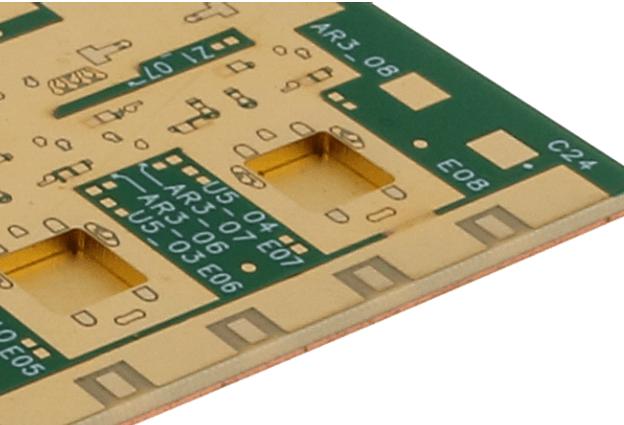
Designing portable high frequency printed circuit boards (PCBs) requires meticulous attention to detail and a comprehensive understanding of various technical aspects. These PCBs are integral to modern electronic devices, particularly those that demand high performance in compact forms, such as smartphones, tablets, and other portable gadgets. The design considerations for these PCBs are multifaceted, encompassing material selection, signal integrity, thermal management, and power efficiency.
To begin with, the choice of materials is paramount in the design of portable high frequency PCBs.
The substrate material must exhibit low dielectric loss and high thermal stability to ensure minimal signal degradation and efficient heat dissipation. Commonly used materials include FR-4, Rogers, and Teflon, each offering distinct advantages. For instance, Rogers materials are preferred for their superior high-frequency performance, while FR-4 is cost-effective and widely available. The selection process involves balancing performance requirements with budget constraints, making it a critical decision in the design phase.
Signal integrity is another crucial consideration.
High frequency signals are susceptible to various forms of interference, including crosstalk, electromagnetic interference (EMI), and signal reflection. To mitigate these issues, designers employ techniques such as controlled impedance routing, differential signaling, and the use of ground planes. Controlled impedance routing ensures that the impedance of the signal traces remains consistent, thereby reducing signal reflections. Differential signaling, on the other hand, involves using pairs of traces to carry signals, which helps in canceling out noise and improving signal integrity. Ground planes act as a shield against EMI, further enhancing the performance of the PCB.
Thermal management is equally important in the design of portable high frequency PCBs.
High frequency components tend to generate significant amounts of heat, which can adversely affect the performance and longevity of the device. Effective thermal management strategies include the use of thermal vias, heat sinks, and thermal interface materials. Thermal vias are small holes filled with conductive material that facilitate heat transfer from the PCB to the heat sink. Heat sinks are attached to the PCB to dissipate heat into the surrounding environment, while thermal interface materials improve the thermal conductivity between the heat-generating components and the heat sink.
Power efficiency is a critical factor, especially for portable devices that rely on battery power.
Designers must ensure that the PCB operates efficiently to prolong battery life. This involves optimizing the power distribution network (PDN) to minimize power losses and ensure stable voltage levels across the PCB. Techniques such as using low-dropout regulators (LDOs), switching regulators, and power gating are commonly employed. LDOs provide a stable output voltage with minimal power loss, while switching regulators are more efficient for higher power applications. Power gating involves selectively turning off parts of the circuit that are not in use, thereby conserving power.
In conclusion, the design of portable high frequency PCBs is a complex process that requires careful consideration of various factors. Material selection, signal integrity, thermal management, and power efficiency are all critical elements that must be addressed to ensure the optimal performance of the PCB. By employing advanced design techniques and leveraging the latest materials and technologies, designers can create high-performance PCBs that meet the demanding requirements of modern portable electronic devices.
Challenges And Solutions In Manufacturing Portable High Frequency PCB
Portable high frequency printed circuit boards (PCBs) are integral components in modern electronic devices, particularly those requiring high-speed data transmission and compact form factors. These PCBs are designed to operate at high frequencies, often in the gigahertz range, making them essential for applications such as wireless communication, radar systems, and advanced computing. However, the manufacturing of portable high frequency PCBs presents several challenges that necessitate innovative solutions to ensure performance, reliability, and cost-effectiveness.
One of the primary challenges in manufacturing portable high frequency PCBs is the selection of suitable materials.
High frequency signals are highly susceptible to losses and interference, which can degrade the performance of the PCB. Therefore, materials with low dielectric constant and low loss tangent are essential to minimize signal attenuation and maintain signal integrity. Traditional materials like FR-4 are often inadequate for high frequency applications, prompting the use of specialized substrates such as PTFE (polytetrafluoroethylene) and ceramic-filled laminates. These materials, while effective, are more expensive and difficult to process, adding complexity to the manufacturing process.
Another significant challenge is the precision required in the fabrication process.
High frequency PCBs demand tight tolerances in trace width, spacing, and layer alignment to ensure consistent impedance and minimize signal reflection. Achieving such precision necessitates advanced manufacturing techniques and equipment, such as laser direct imaging (LDI) and controlled depth drilling. These technologies enable the production of fine features and complex geometries, but they also require significant investment and expertise, which can be a barrier for smaller manufacturers.
Thermal management is also a critical concern in the design and manufacture of portable high frequency PCBs.
High frequency operation generates substantial heat, which can affect the performance and longevity of the PCB. Effective thermal management solutions, such as the use of thermal vias, heat sinks, and advanced cooling techniques, are essential to dissipate heat and maintain optimal operating temperatures. However, integrating these solutions into a compact, portable design without compromising performance or increasing weight is a delicate balancing act.
Moreover, electromagnetic interference (EMI) poses a considerable challenge in high frequency PCB design.
High frequency signals can radiate and couple with other components, leading to unwanted noise and signal degradation. To mitigate EMI, designers employ various shielding techniques, such as ground planes, shielding enclosures, and careful layout strategies. These measures, while effective, can complicate the design process and increase manufacturing costs.
Despite these challenges, several solutions have been developed to enhance the manufacturability and performance of portable high frequency PCBs.
Advances in material science have led to the development of new substrates that offer improved electrical properties and processability. Additionally, innovations in fabrication technology, such as additive manufacturing and advanced photolithography, have enabled greater precision and complexity in PCB designs. Furthermore, simulation and modeling tools have become invaluable in optimizing PCB layouts and predicting performance, allowing designers to address potential issues before fabrication.
In conclusion, the manufacturing of portable high frequency PCBs is fraught with challenges, from material selection and precision fabrication to thermal management and EMI mitigation. However, through the adoption of advanced materials, cutting-edge fabrication techniques, and sophisticated design tools, these challenges can be effectively addressed. As technology continues to evolve, the solutions to these challenges will undoubtedly advance, paving the way for even more powerful and compact electronic devices.


