What is printed circuit board assembly
Introduction To Printed Circuit Board Assembly
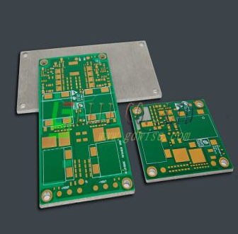
Printed Circuit Board Assembly (PCBA) is a critical process in the manufacturing of electronic devices, serving as the backbone for the functionality of modern electronics. This intricate procedure involves the mounting of various electronic components onto a printed circuit board (PCB), which is a flat, insulating board that provides both mechanical support and electrical connections for the components. The assembly process is essential for transforming a bare PCB into a fully functional electronic circuit, capable of performing the desired operations.
To begin with, the process of PCBA starts with the design and fabrication of the PCB itself.
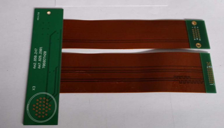
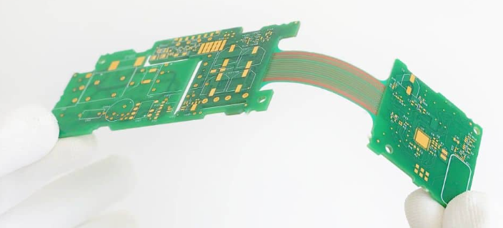
The PCB is typically made from a non-conductive substrate, such as fiberglass or composite epoxy, and is layered with thin copper traces that form the electrical pathways. These pathways are meticulously designed using computer-aided design (CAD) software to ensure precise connections between components. Once the design is finalized, the PCB is manufactured through a series of steps including etching, drilling, and plating, resulting in a board that is ready for component placement.
Following the fabrication of the PCB, the next phase involves the application of solder paste to the board.
Solder paste, a mixture of powdered solder and flux, is applied to the areas where components will be mounted. This is typically done using a stencil that ensures the paste is deposited accurately and uniformly. The application of solder paste is a crucial step, as it facilitates the subsequent soldering process by providing the necessary material to form strong electrical and mechanical bonds between the components and the PCB.
Once the solder paste is in place, the components are positioned onto the PCB.
This is often achieved through automated machines known as pick-and-place machines, which are capable of placing thousands of components per hour with high precision. These machines use vacuum nozzles to pick up components from reels or trays and place them onto the PCB according to the design specifications. The accuracy of this step is paramount, as even slight misalignments can lead to malfunctioning circuits.
After the components are placed, the assembly undergoes a soldering process to secure the components to the PCB.
There are several methods of soldering, with reflow soldering being the most common for surface-mount technology (SMT) components. In reflow soldering, the assembled PCB is passed through a reflow oven where it is gradually heated to melt the solder paste, forming solid solder joints as it cools. For through-hole components, wave soldering or hand soldering may be employed, depending on the complexity and requirements of the assembly.
Following soldering, the assembled PCB is subjected to rigorous inspection and testing to ensure its functionality and reliability.
Automated optical inspection (AOI) systems are used to check for defects such as solder bridges, missing components, or misalignments. Additionally, in-circuit testing (ICT) and functional testing are performed to verify the electrical performance of the assembly. These tests are crucial for identifying any issues that could affect the performance of the final product.
In conclusion, Printed Circuit Board Assembly is a multifaceted process that involves the precise placement and soldering of electronic components onto a PCB. From the initial design and fabrication of the PCB to the final inspection and testing of the assembled board, each step is critical to ensuring the functionality and reliability of electronic devices. As technology continues to advance, the methods and techniques used in PCBA will undoubtedly evolve, further enhancing the capabilities and performance of electronic products.
Key Components In Printed Circuit Board Assembly
Printed circuit board assembly (PCBA) is a critical process in the manufacturing of electronic devices, involving the integration of various components onto a printed circuit board (PCB). This assembly process is essential for the functionality of electronic devices, as it ensures that electrical connections are made between different components, allowing the device to perform its intended functions. To understand the intricacies of PCBA, it is important to explore the key components involved in this process.
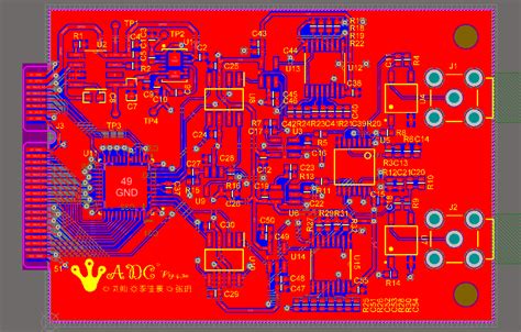
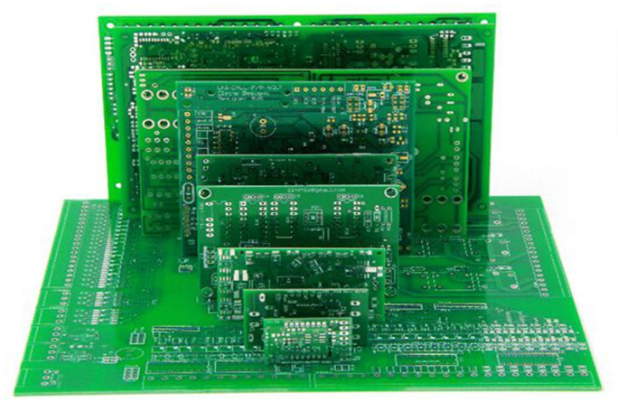
One of the primary components in PCBA is the PCB itself, which serves as the foundation for the entire assembly.
The PCB is typically made of a non-conductive substrate, such as fiberglass, with conductive pathways etched or printed onto its surface. These pathways, often referred to as traces, facilitate the flow of electrical signals between components. The design and layout of the PCB are crucial, as they determine the efficiency and reliability of the final product.
Another essential component in PCBA is the surface mount device (SMD).
SMDs are electronic components that are mounted directly onto the surface of the PCB, as opposed to being inserted into holes. This method of mounting allows for a more compact and efficient design, as it eliminates the need for additional space to accommodate through-hole components. Common SMDs include resistors, capacitors, diodes, and integrated circuits (ICs). These components are typically placed on the PCB using automated machines, which ensure precise placement and alignment.
In addition to SMDs, through-hole components also play a significant role in PCBA.
These components have leads that are inserted into holes drilled into the PCB and soldered in place. Through-hole components are often used for larger or more robust components, such as connectors, transformers, and certain types of capacitors and resistors. While through-hole technology is less common in modern electronics due to its larger footprint, it remains an important aspect of PCBA for specific applications.
The soldering process is another critical element in PCBA, as it ensures that components are securely attached to the PCB and that electrical connections are made.
There are two primary methods of soldering used in PCBA: reflow soldering and wave soldering. Reflow soldering is typically used for SMDs and involves applying solder paste to the PCB, placing the components, and then heating the assembly in a reflow oven. The heat causes the solder paste to melt and form a solid connection between the components and the PCB. Wave soldering, on the other hand, is used for through-hole components and involves passing the PCB over a wave of molten solder, which coats the leads and forms a secure connection.
Furthermore, inspection and testing are vital components of the PCBA process.
After assembly, the PCB must be thoroughly inspected to ensure that all components are correctly placed and soldered. Automated optical inspection (AOI) systems are commonly used for this purpose, as they can quickly and accurately identify any defects or misalignments. Additionally, functional testing is performed to verify that the assembled PCB operates as intended. This may involve applying power to the PCB and measuring various electrical parameters to ensure that the device functions correctly.
In conclusion, printed circuit board assembly is a complex and multifaceted process that involves the integration of various key components. The PCB, surface mount devices, through-hole components, soldering techniques, and inspection and testing procedures all play crucial roles in ensuring the functionality and reliability of electronic devices. Understanding these components and their interactions is essential for anyone involved in the design and manufacturing of electronic products.

The Process Of Printed Circuit Board Assembly
Printed circuit board assembly, often abbreviated as PCBA, is a critical process in the manufacturing of electronic devices. It involves the mounting of various electronic components onto a printed circuit board (PCB) to create a functional electronic circuit. The process of PCBA is intricate and requires precision, as the performance and reliability of the final product depend heavily on the quality of the assembly.
The initial step in the PCBA process is the application of solder paste.
Solder paste, a mixture of tiny solder particles and flux, is applied to the PCB using a stencil. This stencil ensures that the paste is deposited only on the areas where components will be placed. The accuracy of this step is paramount, as it sets the foundation for the subsequent placement of components.
Following the application of solder paste, the next phase involves the placement of electronic components onto the PCB.
This is typically done using automated machines known as pick-and-place machines. These machines are programmed to pick components from reels or trays and place them precisely onto the PCB. The components can range from tiny resistors and capacitors to larger integrated circuits and connectors. The precision of the pick-and-place machines ensures that each component is placed accurately, which is crucial for the functionality of the final product.
Once the components are placed, the assembly moves to the soldering stage.
There are two primary methods of soldering in PCBA: reflow soldering and wave soldering. Reflow soldering is commonly used for surface-mount technology (SMT) components. In this method, the PCB with the placed components is passed through a reflow oven. The oven heats the board to a temperature that melts the solder paste, creating a strong bond between the components and the PCB. On the other hand, wave soldering is used for through-hole components. In this method, the PCB is passed over a wave of molten solder, which adheres to the exposed metal areas and forms a secure connection.
After soldering, the assembled PCB undergoes inspection and testing to ensure that it functions correctly.
Automated optical inspection (AOI) systems are often used to check for defects such as misaligned components, insufficient solder, or solder bridges. Additionally, X-ray inspection may be employed to examine solder joints that are not visible to the naked eye, particularly for components with hidden connections like ball grid arrays (BGAs).
Functional testing is another critical step in the PCBA process.
This involves applying power to the assembled PCB and running a series of tests to verify that it operates as intended. Any issues identified during testing are addressed through rework, where technicians manually correct defects or replace faulty components.
Finally, the assembled and tested PCBs are cleaned to remove any residual flux or contaminants that could affect performance. This is typically done using specialized cleaning agents and equipment. The cleaned PCBs are then ready for integration into the final product.
In conclusion, the process of printed circuit board assembly is a complex and meticulous procedure that involves several stages, from solder paste application to final testing and cleaning. Each step is crucial in ensuring the reliability and functionality of the electronic devices we rely on daily. The advancements in automation and inspection technologies have significantly improved the efficiency and accuracy of PCBA, making it possible to produce high-quality electronic products at scale.
Common Challenges In Printed Circuit Board Assembly
Printed circuit board assembly (PCBA) is a critical process in the manufacturing of electronic devices, involving the mounting of electronic components onto a printed circuit board (PCB). Despite its importance, the assembly process is fraught with numerous challenges that can impact the quality, reliability, and performance of the final product.
One of the most common challenges in PCBA is component placement accuracy.
As electronic devices become increasingly compact, the components used in these devices also shrink in size. This miniaturization demands precise placement of components on the PCB, which can be difficult to achieve consistently. Even a slight misalignment can lead to malfunctioning circuits or complete device failure.
Another significant challenge is soldering quality.
Soldering is the process of joining electronic components to the PCB using a molten metal alloy. Poor soldering can result in weak joints, which may break under mechanical stress or thermal cycling. Additionally, soldering defects such as cold joints, solder bridges, and voids can compromise the electrical integrity of the circuit. Ensuring high-quality soldering requires meticulous control of temperature, solder paste application, and reflow profiles, which can be difficult to maintain consistently in a high-volume production environment.
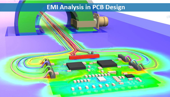
Thermal management is also a critical concern in PCBA.
Electronic components generate heat during operation, and if this heat is not effectively dissipated, it can lead to overheating and subsequent failure of the device. Designing PCBs with adequate thermal management features, such as heat sinks, thermal vias, and proper component spacing, is essential. However, achieving optimal thermal performance often involves trade-offs with other design considerations, such as signal integrity and mechanical stability.
Furthermore, the increasing complexity of electronic devices poses a challenge in terms of testing and inspection.
Ensuring that a PCB is free from defects and functions as intended requires comprehensive testing, including in-circuit testing (ICT), functional testing, and automated optical inspection (AOI). These testing methods can be time-consuming and costly, particularly for complex boards with a high density of components. Moreover, identifying and diagnosing faults in densely packed PCBs can be challenging, necessitating advanced diagnostic tools and skilled technicians.
Supply chain management is another area where challenges frequently arise.
The global nature of the electronics industry means that components are often sourced from multiple suppliers across different regions. This can lead to issues with component availability, lead times, and quality control. Additionally, the risk of counterfeit components entering the supply chain is a growing concern, as these can compromise the reliability and safety of the final product. Effective supply chain management requires robust supplier vetting processes, stringent quality control measures, and contingency planning to mitigate the impact of supply disruptions.
Lastly, regulatory compliance is an ongoing challenge in PCBA.
Electronic devices must adhere to various industry standards and regulations, such as RoHS (Restriction of Hazardous Substances) and REACH (Registration, Evaluation, Authorization, and Restriction of Chemicals). Compliance with these regulations often necessitates changes in materials, processes, and documentation, which can be both time-consuming and costly. Staying abreast of evolving regulatory requirements and ensuring that all aspects of the assembly process are compliant is essential to avoid legal and financial repercussions.
In conclusion, printed circuit board assembly is a complex process that involves numerous challenges, from component placement accuracy and soldering quality to thermal management, testing, supply chain management, and regulatory compliance. Addressing these challenges requires a combination of advanced technology, skilled personnel, and robust processes to ensure the production of high-quality, reliable electronic devices.