What is rf pcb design
Introduction To RF PCB Design: Key Concepts And Principles
RF PCB design, or Radio Frequency Printed Circuit Board design, is a specialized area within the broader field of PCB design that focuses on the unique challenges and requirements associated with high-frequency signals. As electronic devices become more sophisticated and wireless communication becomes increasingly prevalent, the demand for effective RF PCB design has grown significantly. Understanding the key concepts and principles of RF PCB design is essential for engineers and designers who aim to create reliable and efficient high-frequency circuits.
One of the fundamental aspects of RF PCB design is the management of signal integrity.
At high frequencies, signals are more susceptible to various forms of interference and degradation, such as crosstalk, electromagnetic interference (EMI), and signal reflection. To mitigate these issues, designers must carefully consider the layout and routing of traces on the PCB. For instance, maintaining consistent trace impedance is crucial to minimize signal reflection and ensure signal integrity. This often involves using controlled impedance traces, which require precise calculations and careful material selection.
Another critical principle in RF PCB design is the use of proper grounding techniques.
A well-designed ground plane can significantly reduce noise and improve the overall performance of the circuit. Ground planes provide a low-impedance path for return currents, which helps to minimize EMI and crosstalk. Additionally, they can act as a shield to protect sensitive components from external interference. Designers must ensure that the ground plane is continuous and free of gaps, as discontinuities can lead to unwanted resonances and signal degradation.
Component placement is also a vital consideration in RF PCB design.
The physical location of components on the PCB can have a significant impact on the performance of the circuit. For example, placing sensitive components too close to high-frequency signal traces can result in unwanted coupling and interference. To avoid this, designers should group components with similar functions together and keep high-frequency components isolated from low-frequency ones. Furthermore, minimizing the length of signal paths can help reduce signal loss and improve overall performance.
The choice of materials is another important factor in RF PCB design.
The dielectric properties of the substrate material can affect the propagation of high-frequency signals. Materials with low dielectric constant (Dk) and low loss tangent (Df) are typically preferred for RF applications, as they help to minimize signal loss and maintain signal integrity. Common materials used in RF PCB design include PTFE (Teflon), Rogers, and other specialized high-frequency laminates.
Thermal management is also a key consideration in RF PCB design.
High-frequency circuits can generate significant amounts of heat, which can affect the performance and reliability of the components. Effective thermal management strategies, such as the use of thermal vias, heat sinks, and proper airflow, are essential to ensure that the circuit operates within safe temperature limits.
In conclusion, RF PCB design is a complex and specialized field that requires a deep understanding of high-frequency signal behavior and the implementation of various design principles to ensure signal integrity, minimize interference, and maintain overall circuit performance.
By carefully considering factors such as trace impedance, grounding techniques, component placement, material selection, and thermal management, designers can create reliable and efficient RF circuits that meet the demands of modern wireless communication and electronic devices. As technology continues to advance, the importance of effective RF PCB design will only continue to grow, making it an essential skill for engineers and designers in the electronics industry.
Essential Components And Materials For RF PCB Design
RF PCB design, or Radio Frequency Printed Circuit Board design, is a specialized area within the broader field of PCB design that focuses on the unique requirements of high-frequency signal transmission. The essential components and materials used in RF PCB design are critical to ensuring optimal performance, signal integrity, and reliability. Understanding these elements is fundamental for engineers and designers working in this domain.
To begin with, the choice of substrate material is paramount in RF PCB design.
Unlike standard PCBs, which often use FR-4 material, RF PCBs typically require substrates with lower dielectric constants and lower loss tangents. Materials such as Rogers, Taconic, and PTFE (Polytetrafluoroethylene) are commonly used due to their superior electrical properties. These materials help minimize signal loss and maintain signal integrity at high frequencies, which is crucial for RF applications.
In addition to substrate materials, the selection of copper cladding is another critical consideration.
The thickness and type of copper used can significantly impact the performance of the RF PCB. Thinner copper layers are often preferred for high-frequency applications to reduce skin effect losses, where high-frequency currents tend to flow on the surface of the conductor. Moreover, smooth copper surfaces are advantageous as they reduce signal attenuation and improve overall performance.
The design of transmission lines is another essential aspect of RF PCB design.
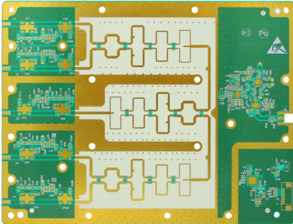
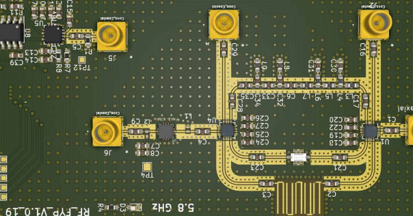
Microstrip and stripline are the two most common types of transmission lines used. Microstrip lines are placed on the outer layer of the PCB, with a ground plane on the opposite side, while stripline transmission lines are sandwiched between two ground planes within the PCB. The choice between microstrip and stripline depends on the specific application and design requirements. Both types require precise control of impedance, which is achieved through careful design of the trace width, spacing, and the dielectric properties of the substrate.
Furthermore, the layout and placement of components play a crucial role in RF PCB design.
Components such as capacitors, inductors, and resistors must be strategically placed to minimize parasitic effects and signal interference. The use of surface-mount technology (SMT) components is often preferred over through-hole components due to their smaller size and better performance at high frequencies. Additionally, the placement of components should be optimized to reduce the length of signal paths and avoid unnecessary bends and vias, which can introduce signal reflections and losses.
Grounding and shielding are also vital considerations in RF PCB design.
A solid and continuous ground plane is essential to provide a low-impedance return path for high-frequency signals and to minimize electromagnetic interference (EMI). In some cases, additional shielding may be required to protect sensitive components from external noise and to prevent the emission of RF signals that could interfere with other devices.
Lastly, the use of advanced simulation and modeling tools is indispensable in RF PCB design.
These tools allow designers to predict the behavior of the PCB under various conditions and to optimize the design before fabrication. Electromagnetic simulation software can model the effects of different materials, trace geometries, and component placements, enabling designers to make informed decisions and achieve the desired performance.
In conclusion, RF PCB design involves a careful selection of materials, precise transmission line design, strategic component placement, effective grounding and shielding, and the use of advanced simulation tools. Each of these elements is crucial to ensuring the successful design and performance of RF PCBs, which are integral to a wide range of high-frequency applications.
Common Challenges And Solutions In RF PCB Design
RF PCB design, or Radio Frequency Printed Circuit Board design, is a specialized area within the broader field of PCB design that focuses on the unique requirements of high-frequency signal transmission. This domain presents a set of challenges that are distinct from those encountered in low-frequency or digital PCB design. Understanding these challenges and their corresponding solutions is crucial for engineers aiming to create efficient and reliable RF circuits.
One of the primary challenges in RF PCB design is signal integrity.
At high frequencies, even minor imperfections in the PCB layout can lead to significant signal degradation. This is due to the fact that RF signals are highly susceptible to interference and loss. To mitigate this, designers must pay meticulous attention to the layout, ensuring that signal paths are as short and direct as possible. Additionally, the use of controlled impedance traces is essential. Controlled impedance helps maintain signal integrity by ensuring that the characteristic impedance of the trace matches the impedance of the source and load, thereby minimizing reflections and signal loss.
Another significant challenge is managing electromagnetic interference (EMI).
RF circuits can both emit and be affected by EMI, which can lead to performance issues or even complete circuit failure. Shielding is a common solution to this problem. By enclosing sensitive components in a conductive material, designers can prevent external EMI from affecting the circuit. Furthermore, proper grounding techniques are vital. A well-designed ground plane can act as a shield and provide a low-impedance path for return currents, thereby reducing EMI.
Thermal management is also a critical concern in RF PCB design.
High-frequency components often generate substantial amounts of heat, which can affect performance and reliability. Effective thermal management strategies include the use of thermal vias, heat sinks, and careful placement of components to ensure adequate heat dissipation. Thermal vias are particularly useful as they provide a path for heat to move from the top layer of the PCB to the bottom layer, where it can be dissipated more effectively.
Component selection poses another challenge.
RF circuits require components that can operate efficiently at high frequencies. This includes not only active components like transistors and amplifiers but also passive components such as capacitors, inductors, and resistors. These components must have low parasitic elements, which are unintended inductances and capacitances that can affect performance at high frequencies. Choosing components with appropriate specifications and placing them correctly on the PCB can significantly enhance the overall performance of the RF circuit.
Moreover, the choice of PCB material is crucial in RF design.
Standard FR4 material, commonly used in low-frequency designs, may not be suitable for high-frequency applications due to its higher dielectric losses. Instead, materials like Rogers or Teflon, which have lower dielectric constants and loss tangents, are often preferred. These materials help maintain signal integrity by reducing signal loss and ensuring consistent performance across the frequency range.
In conclusion, RF PCB design is fraught with challenges that require specialized knowledge and techniques to overcome. Signal integrity, EMI management, thermal management, component selection, and material choice are all critical factors that must be carefully considered. By addressing these challenges with appropriate solutions, designers can create RF circuits that are both efficient and reliable, ensuring optimal performance in high-frequency applications.
Advanced Techniques For Optimizing RF PCB Performance
RF PCB design, or Radio Frequency Printed Circuit Board design, is a specialized field that focuses on the creation of circuit boards capable of handling high-frequency signals. These signals, typically in the range of 3 kHz to 300 GHz, are used in various applications such as wireless communication, radar systems, and satellite technology. Given the complexity and sensitivity of RF signals, optimizing RF PCB performance requires advanced techniques that go beyond standard PCB design practices.
One of the primary considerations in RF PCB design is impedance control.
Impedance mismatches can lead to signal reflections, which degrade the performance of the circuit. To mitigate this, designers must carefully calculate and control the impedance of transmission lines. This involves selecting appropriate materials with consistent dielectric properties and designing trace geometries that maintain the desired impedance. Techniques such as microstrip and stripline configurations are commonly employed to achieve precise impedance control.
Another critical aspect is the minimization of signal loss.
High-frequency signals are particularly susceptible to losses due to the skin effect, where the signal tends to travel along the surface of the conductor, increasing resistance. To address this, designers often use materials with lower loss tangents and high conductivity, such as copper with a smooth finish. Additionally, the use of shorter trace lengths and wider traces can help reduce signal attenuation.
Electromagnetic interference (EMI) and crosstalk are also significant challenges in RF PCB design.
EMI can originate from various sources, including other electronic components and external devices. To minimize EMI, designers employ shielding techniques such as ground planes and metal enclosures. Ground planes not only provide a return path for signals but also act as a shield against external noise. Furthermore, proper spacing between traces and the use of guard traces can help reduce crosstalk, which is the unwanted coupling of signals between adjacent traces.
Thermal management is another crucial factor in optimizing RF PCB performance.
High-frequency circuits often generate significant heat, which can affect the reliability and performance of the components. Effective thermal management strategies include the use of thermal vias, heat sinks, and thermal pads to dissipate heat away from critical areas. Additionally, selecting materials with high thermal conductivity can help improve heat dissipation.
Component placement and routing are equally important in RF PCB design.
Placing components too close to each other can lead to unwanted parasitic effects, while improper routing can introduce additional inductance and capacitance, affecting signal integrity. To optimize performance, designers must follow best practices such as maintaining consistent trace widths, avoiding sharp bends, and using differential pairs for high-speed signals. Additionally, the use of simulation tools can help identify potential issues and optimize the layout before fabrication.
Finally, testing and validation are essential steps in ensuring the optimized performance of RF PCBs.
Techniques such as Time Domain Reflectometry (TDR) and Vector Network Analysis (VNA) are used to measure impedance, signal integrity, and other critical parameters. These tests help identify any discrepancies between the designed and actual performance, allowing for necessary adjustments.
In conclusion, optimizing RF PCB performance requires a comprehensive approach that addresses impedance control, signal loss minimization, EMI and crosstalk reduction, thermal management, and precise component placement and routing. By employing these advanced techniques, designers can create RF PCBs that meet the stringent requirements of high-frequency applications, ensuring reliable and efficient operation.


