What is the Green Mask Plugging Process in PCB Manufacturing?
Introduction to PCB Green Mask and Via Plugging
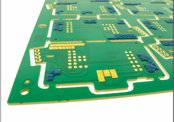
Printed Circuit Board (PCB) manufacturing involves numerous intricate processes that contribute to the final product’s functionality and reliability. Among these processes, the application of solder mask (commonly referred to as “green mask” due to its traditional color) and via plugging play critical roles in modern PCB production. The green mask plugging process, specifically, has become increasingly important as electronic devices continue to shrink in size while growing in complexity.
This article will provide a comprehensive examination of the green mask plugging process in PCB manufacturing, covering its purpose, techniques, advantages, challenges, and applications in today’s electronics industry.
Understanding PCB Solder Mask (Green Mask)
Definition and Purpose of Solder Mask
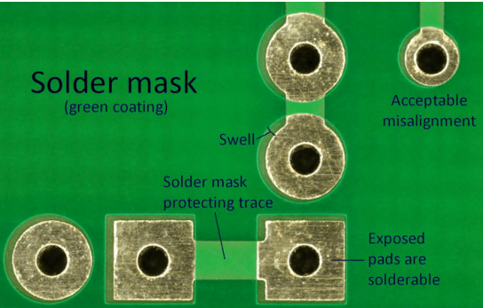
Solder mask, often called “green mask” because of its most common color (though it’s available in other colors like red, blue, or black), is a thin lacquer-like layer of polymer applied to the copper traces of a PCB. Its primary purposes include:
- Preventing solder bridges from forming between closely spaced solder pads during assembly
- Protecting copper traces from oxidation and environmental damage
- Providing electrical insulation between conductors
- Offering mechanical protection to the circuitry
- Improving the PCB’s aesthetics and readability through contrast with silkscreen markings
Composition of Solder Mask
Modern solder mask materials typically consist of:
- Resin systems (usually epoxy-based)
- Photoactive compounds for UV curing
- Pigments (typically green, but other colors are available)
- Fillers to modify physical properties
- Solvents to adjust viscosity for application
The exact formulations vary between manufacturers and are often proprietary, designed to meet specific performance requirements.
The Need for Via Plugging in PCBs
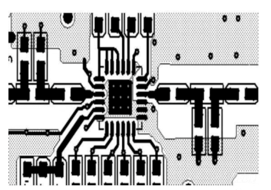
What are Vias in PCBs?
Vias are plated through-holes (PTH) that provide electrical connections between different layers of a multilayer PCB. They come in several types:
- Through-hole vias: Span the entire board thickness
- Blind vias: Connect an outer layer to one or more inner layers
- Buried vias: Connect only inner layers without reaching the surface
Challenges with Unplugged Vias
Unplugged vias can present several problems in PCB assembly and operation:
- Solder wicking: During assembly, solder can flow into vias, potentially starving the intended solder joint
- Contamination: Vias can trap flux residues and cleaning solutions
- Airflow blockage: In pressurization or conformal coating processes
- Planarity issues: For surface mount components, especially with fine pitch devices
- Moisture entrapment: Leading to potential reliability issues
Green Mask Plugging Process Explained
Definition of Green Mask Plugging
Green mask plugging refers to the process of filling via holes with the same material used for the solder mask (typically the green-colored liquid photoimageable solder mask or LPI). This differs from other via filling methods that might use conductive or non-conductive epoxy resins specifically formulated for via filling.
Process Steps
The green mask plugging process typically follows these steps:
- PCB preparation: The board undergoes cleaning to remove contaminants that might affect adhesion
- Via plugging application: The solder mask material is applied to fill the vias using one of several methods (discussed below)
- Excess material removal: The board is treated to remove solder mask from surfaces while leaving it in the vias
- Pre-curing: A partial cure stabilizes the material before imaging
- Exposure: UV light exposes the solder mask through a photomask to define the pattern
- Development: Unexposed areas are washed away, revealing copper pads
- Final curing: A thermal process fully hardens the solder mask
Application Methods for Green Mask Plugging
Several techniques exist for applying the solder mask material into vias:
- Screen printing: Traditional method using a squeegee to force material through a screen
- Curtain coating: The PCB passes through a curtain of flowing solder mask material
- Spray coating: Atomized solder mask is sprayed onto the board surface
- Electrostatic coating: Uses electrical charges to improve material deposition
- Vacuum plugging: Creates suction to draw material into vias
Screen printing remains the most common method for green mask plugging, particularly for larger via sizes.

Advantages of Green Mask Plugging
Cost Effectiveness
Using the same material for both solder mask and via plugging offers significant cost advantages:
- Eliminates need for separate via fill materials
- Reduces process steps compared to dedicated via fill processes
- Utilizes existing solder mask application equipment
Process Simplicity
Green mask plugging integrates well with standard PCB fabrication flows:
- Performed during normal solder mask application
- Doesn’t require additional curing steps beyond normal solder mask processing
- Compatible with existing imaging and development processes
Adequate Performance for Many Applications
For many standard PCB applications, green mask plugging provides sufficient:
- Surface planarity for component placement
- Protection against contamination
- Prevention of solder wicking
- Basic environmental protection
Limitations and Considerations
Material Properties
Solder mask materials have certain limitations when used for via plugging:
- Thermal properties: Typically lower thermal conductivity than dedicated via fill materials
- CTE mismatch: May have different coefficient of thermal expansion than the PCB substrate
- Curing shrinkage: Can lead to minor depression or dimpling over vias
- Moisture absorption: Generally higher than specialized via fill materials
Via Size Limitations
Green mask plugging works best with certain via characteristics:
- Diameter: Typically most effective for vias between 0.2mm and 0.5mm
- Aspect ratio: Generally limited to depth:diameter ratios below 4:1 for reliable plugging
- Via shape: Works best with straight-walled, laser-drilled vias
Reliability Considerations
For high-reliability applications, green mask plugging may not be suitable when:
- Hermetic sealing is required
- Extreme thermal cycling is expected
- Very low moisture absorption is needed
- High thermal conductivity is essential
Comparison with Other Via Filling Methods
Conductive Epoxy Filling
Used when electrical or thermal conductivity is needed through the via:
- More expensive than green mask plugging
- Requires specialized application and curing
- Provides better thermal management
- Used for thermal vias or when grounding is critical
Non-Conductive Epoxy Filling
Offers superior performance for demanding applications:
- Lower moisture absorption
- Better thermal stability
- Reduced curing shrinkage
- More reliable in harsh environments
- Higher cost than green mask plugging
Copper Filling
Provides the highest performance but at greatest cost:
- Complete electrical and thermal conductivity
- Maximum reliability
- Complex electrochemical process required
- Used in high-power or high-frequency applications
Process Control and Quality Assurance
Key Parameters to Monitor
Successful green mask plugging requires careful control of:
- Material viscosity: Affects filling capability and surface coverage
- Application method: Must ensure complete via filling without voids
- Curing profile: Temperature and time affect final material properties
- Via preparation: Cleanliness and surface condition impact adhesion
- Environmental conditions: Temperature and humidity during processing
Inspection Methods
Several techniques verify proper green mask plugging:
- Visual inspection: Under magnification for complete filling and surface condition
- Cross-sectioning: Destructive testing to examine fill quality
- Automated optical inspection (AOI): For surface defects and coverage
- Electrical testing: For continuity where appropriate
- Thermal imaging: To detect voids in some cases
Common Defects and Solutions
Typical green mask plugging issues include:
- Incomplete filling: Adjust material viscosity or application parameters
- Voids: Improve vacuum conditions if used, or material degassing
- Surface dimples: Optimize curing profile to reduce shrinkage
- Adhesion failure: Enhance via cleaning and surface preparation
- Cracking: Modify material selection or thermal profile
Applications of Green Mask Plugging
Consumer Electronics
Ideal for cost-sensitive, high-volume products:
- Smartphones and tablets
- Home appliances
- Entertainment systems
- Wearable devices
Industrial Electronics
Suitable for many industrial control applications:
- PLCs and automation controllers
- Sensors and instrumentation
- Power supplies
- Human-machine interfaces
Automotive Electronics
Used in non-critical automotive applications:
- Infotainment systems
- Body control modules
- Interior lighting controls
- Non-safety-related functions
LED Lighting
Common in PCB-based lighting solutions:
- LED arrays
- Light strips
- Decorative lighting
- Signage
Future Trends in Green Mask Plugging
Material Developments
Ongoing improvements in solder mask formulations may enhance plugging capabilities:
- Lower shrinkage materials
- Reduced moisture absorption
- Improved thermal stability
- Higher reliability formulations
Process Innovations
Emerging technologies may improve green mask plugging:
- More precise application methods
- Better void detection systems
- Advanced curing technologies
- Automated process control
Expanding Applications
As materials improve, green mask plugging may find use in more demanding applications:
- Higher reliability consumer products
- Selected automotive applications
- Certain aerospace subsystems
- Industrial IoT devices
Conclusion
The green mask plugging process in PCB manufacturing offers a cost-effective and efficient solution for via filling in many electronic applications. By utilizing the same material used for solder mask application, this process simplifies production while providing adequate protection and performance for a wide range of products. While it may not be suitable for the most demanding applications requiring specialized via fill materials, green mask plugging remains a vital technique in the PCB fabricator’s toolkit, particularly for high-volume, cost-sensitive consumer electronics.
As PCB technology continues to evolve with smaller features and higher densities, the green mask plugging process will likely see continued refinement to meet these challenges while maintaining its economic advantages. Understanding this process is essential for PCB designers and engineers to make informed decisions about via treatment options that balance performance, reliability, and cost in their specific applications.