What is the standard for PCB warpage?
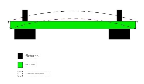
PCB warpage actually refers to the bending of the circuit board. It means that the originally flat circuit board will be slightly warped at both ends or in the middle when placed on the desktop. This phenomenon is called PCB warpage by industry insiders.
The circuit board warpage calculation formula is to place the circuit board flat on the desktop with the four corners of the circuit board touching the ground and measure the height of the arch in the middle. The calculation method is: Warpage = Height of arch/Length of the long side of the PCB*100%.
Industry standard for circuit board warpage: According to the American IPC-6012 (1996 edition) “Qualification and Performance Specifications for Rigid Printed Boards”, the maximum warpage and distortion allowed for the production of circuit boards is between 0.75% and 1.5%. Because the process capabilities of each factory are different, there are also certain differences in the requirements for PCB warpage control. For conventional double-sided multi-layer circuit boards with a thickness of 1.6, most circuit board manufacturers control the PCB warpage between 0.70-0.75%. Many SMT and BGA boards require it to be within the range of 0.5%. Some circuit board factories with strong process capabilities can increase the PCB warpage standard to 0.3%.

How to avoid circuit board warping during manufacturing
① The semi-cured arrangement between each layer should be symmetrical. For a six-layer circuit board, the thickness between 1-2 and 5-6 layers and the number of semi-cured sheets should be consistent;
② The multi-layer PCB core board and the cured sheet should use products from the same supplier;
③ The circuit pattern area of the outer layer A surface and B surface should be as close as possible. When the A surface is a large copper surface and the B surface has only a few lines, it is easy to cause warping after etching.
How to prevent circuit board warping
- Engineering design: the arrangement of prepregs between layers should correspond; the core board and prepregs of multilayer boards should use the same supplier’s products; the graphics area of the outer C/S surface should be as close as possible, and independent grids can be used;
- Bake the board before unloading: generally 150 degrees for 6-10 hours to remove moisture in the board, further cure the resin completely, and eliminate stress in the board; bake the board before cutting, whether it is the inner layer or both sides!
- Before laminating multilayer boards, pay attention to the warp and weft directions of the board curing sheets: the shrinkage ratios in the warp and weft directions are different. Pay attention to the warp and weft directions before unloading the prepregs; pay attention to the warp and weft directions when unloading the core board; the general board curing sheet roll direction is the warp direction; the long direction of the copper clad board is the warp direction; 10-layer 4OZ power thick copper board
- Lamination thickness eliminates stress After pressing the plate, cold press and trim the burrs;
- Bake the plate before drilling: 150 degrees for 4 hours;
- Thin plates should not be mechanically brushed, and chemical cleaning is recommended; special clamps are used during electroplating to prevent the plate from bending and folding
- After tin spraying, naturally cool it to room temperature on a flat marble or steel plate or cool it on an air flotation bed before cleaning;