What Issues Should Be Considered in PCB Design?
With the booming PCB industry ,more and more engineers and technicians are joining the ranks of PCB design and manufacturing.However,due to the wide range of areas involved in PCB manufacturing,and the fact that a significant number of PCB design engineers(layout personnel)have no experience in or involvement in PCB manufacturing,and the fact that a significant number of PCB design engineer (layout personnel)have no experience in or involvement in PCB manufacturing,the design process often focuses heavily on electrical performance and product functionality.However ,when downstream PCB fabricators receive orders and undergo actual production,many issues arise due to design considerations that lead to manufacturing difficulties,extended processing cycles,or potential product defects.
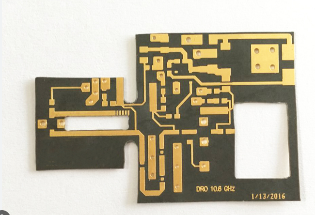
For ease of presentation,this analysis foucuses on seven aspects:cutting ,drilling,routing ,solder mask,marking,surface treatment,and forming.
1.When cutting,the main considerations are board thickness and copper thickness :
For board thicker than 0.8mm,the standard range is:1.0,1.2,1.6,2.0,3.2mm,Board thinner than 0.8mm are not considered standard.Thickness can be determined based on needs,but commonly used thickness include:0.1,0.15,0.2,0.3,0.1,and 0.6mm.These material are primarily used for the inner layers of multilayer boards.\
When designing the outer layer,consider the thickness of the board.Production processing requires additional copper plating,solder mask ,surface treatment(such as tinning,gold plating),and the thickness of the metal plate will be 0.05-0.1mm.For example, if the design requires a 2.0mm thickness,the normal 2.0mm sheet material will be uesd. Considering sheet material and processing tolerances,the finished board thickness will be between 2.1-2.3mm.If the design requires a thickness of no greater than 2.0mm,the board shoud be made from unconventional 1.9mm material .The PCB fabricator will need to place orders from the board manufacturer on short notice,which will significantly increase the lead time.
During inner layer fabrication,the thickness of the laminated board cna be adjusted by adjusting the thickness and structual configuration of the prepreg(PP).This allows for greater flexibility if the finished board thickness requirement is 1.6mm,the core board(core board)can be either 1.2mm or 1.0mm.As long as the laminated board thickness is within a certain range,the required thickness can be met.
Another issue is board thickness tolerance.PCB designers must consider both product assembly tolerance and the post-PCB thickness tolerance.Three factors primarily influence finished product tolerances:incoming board material tolerance,lamination tolerance, and outer layer thickening tolerance.Several common board tolerances are provided for reference:(0.8-1.0) ±0.1, (1.2-1.6) ±0.13, 2.0 ±0.18, and 3.0 ±0.23. Lamination tolerances vary depending on the number of layer and board thickness, and are controlled withing a range of ±0.05-0.1mm. Especially for boards with edge connectors (such as printed circuit boards), the board thickness and tolerance must be determined based on the connector’s matching requirements.
Regarding surface copper thickness,since the copper in the hole is deposited through electroless copper deposition and electroplating, if special treatment is not performed,the surface copper is thickened.According to the IPC-A-600G standard, the minimum copper plating thickness is 20μm for grades 1 and 2, and 25μm for grade 3. Therefore, when manufacturing a circuit board, if the copper thickness requires 1OZ (minimum 30.9μm), the board is sometimes cut to HOZ (minimum 15.4μm) based on the line width/line spacing. Excluding the 2-3μm allowable tolerance, the minimum thickness can reach 33.4μm. If 1OZ is selected, the minimum finished copper thickness will reach 47.9μm. The calculation of other copper thicknesses can be similarly applied.
II.Drilling primarily involves considerations such as hole diameter tolerance,pre-sizing,handing of hole to the board edge,non-plated-hole(PTH)holes,and pilot hole design.
Currently,the smallest drill tip for mechanical drilling is 0.2mm.However,due to the thickness of the copper wall and protective layer,the designed hole diameter must be increased during production.For tin-sprayed PCBs,the diameter must be increased by 0.15mm,and for gold-sprayed PCBs,by0.1mm.The key question here is:if the hole diameter is increased,will the distance from the hole to the circuit and copper foil meet the processing requirement?Will the solder ring around the originally designed circuit pad be sufficient?For example, if the via hole diameter is designed to be 02mm and the pad diameter is 0.35mm,theoretical calculations show that a 0.075mm solder ring on each side is fully processable.However,when the drill tip is increased for tinsprayed PCBs,no solder ring is present.If the CAM engineer cannot increase the pad spacing,the board cannot be processed.
Aperture tolerance: Currently,most domestic drilling rigs maintain a drilling tolerance of ±0.05mm. Considering the tolerance of the plating thickness within the hole,the tolerance for plated holes is ±0.075mm, and for non-plated holes, ±0.05mm.
Another often overlooked issue is the clearance between the drilled hole and the inner copper or trace of a multilayer board.Because the drilling positioning tolerance is ±0.075mm, the deformation of the internal laminated pattern during lamination can result in a ±0.1mm tolerance. Therefore, when designing, ensure the clearance between the hole edge and the trace or copper is at least 0.15mm for four-layer boards and at least 0.2mm for six- or eight-layer boards for convenient production.
Non-plated holes are commonly created using three methods:dry film sealing or via plugging.This allows the plated copper inside the hole to be removed during etching because it lacks corrosion resistance.Pay attention to dry film sealing.Hole diameters should not exceed 6.0mm,and vias plugged with plastic should not be less than 11.5mm. Alternatively,use secondary drilling to create non-plated holes. Regardless of the method used,ensure there is no copper foil within a 0.2mm radius around the non-plated hole.
Register hole design is often overlooked.During circuit board processing,testing,external punching,or electric milling,holes larger than 1.5mm are required for board fixing,When designing,consider distributing the holes in a triangular pattern,preferably at the three corners of the board.
3.Circuit Fabrication:Mainly Consider the impact of Circuit Etching
Due to the impact of undercutting,copper thickness and different processing techniques must be considered during production. Preroughening of the circuit is necessary,considering copper thickness and different processing techniques.For HOZ copper on tinned and immersion gold boards,a typical compensation is 0.025mm,and for 1oz copper,a typical line width/line spacing production capacity is 0.075/0.075mm.Therefore,when considering the minimum line width/line spacing during design,it is important to consider compensation during production.
Since gold-plated board don’t need to remove the gold plating from the circuit after etching,the line width remains unchanged,so compensation is not required.However,due to the presence of undercutting,the copper trace width beneath the gold layer will be smaller than the gold trace width.Excessive copper thickness or excessive etching can easily cause the gold surface to collapse,leading to soldering problems.
For trance with characteristic impedance requirements,the line width/line spacing requirements are even more stringent.
Fourth,the solder mask treatment for vias is particularly challenging:
Because vias not only conduct electricity,many pcb designers use them as in-circuit test points after component assembly,and even rarely as component insertion with oil to prevent soldering.For test points or insertion holes,a window is required.
However,covering vias with tin-sprayed PCBs can easily lead to tin bead trapped in the holes.Therefore,many product use via plugging as a treatment.This is also done to facilitate BGA placement.However,when the hole diameter is lager than 0.6mm,it becomes more difficult to fill the hole with oil(incomplete filing).Therefore,some tin-spraying boards are designed with a semi-open window,with a single side 0.065mm larger than the hole diameter.Tin is sprayed within a 0.065mm range on the hole wall and edge.
5.When processing characters,the main consideration is the addition of solder pads and related marking on the characters.
With increasingly dense component layouts,and the need to avoid printing characters on solder pads when printing characters,ensuring at least a 0.15mm distance between the characters and the pads,the component box and component symbol sometimes cannot be completely distributed on the circuit board.Fortunately,most patching is now completed by machine.Therefore,if adjustment are truly unavoidable during design,consider printing only the character box and omitting the component symbol.
Common marking include supplier logos,UL certification marks,flame retardant ratings,anti-static marking,production cycles,and customer-specified marking.The meaning of each mark must be clearly understood,and it is best to reserve and designate specific placement locations.
6.The impact of PCB surface coating(plating)on design:
Currently,the most widely used surface treatments incude OSP(on-strip printing),gold plating,immersion gold plating,and tin spraying.
We can compare their advantages and disadvantages base on cost,solderability,wear resistance,oxidation resistance,and differences in production processes,drilling,and trace modification.
OSP:Low cost,good conductivity,and planarity. but poor oxidation resistance and storage. Drilling compensation is typically 0.1mm,and HOZ copper thickness and line width compensation is 0.025mm.Due to its high susceptibility to oxidation and dust,OSP processing is performed after forming and cleaning.For single-piece sizes less than 80mm,delivery as connected pieces should be considered.
Electroplated nickel-gold:Excellent oxidation resistance and wear resistance.For plugs or contacts,the gold layer thickness is 1.3µm or greater. For soldering, the gold layer thickness is typically 0.05-0.1µm, but solderability is relatively poor.Drill hole compensation is 0.1mm,and line width compensation is not appliedNote that when manufacturing gold boards with copper thicknesses over 1oz, the copper layer beneath the surface gold layer can easily collapse due to over-etching, leading to solderability issues. Because gold plating requires current assistance, the gold plating process is designed to precede etching. This completes the surface preparation and also acts as an etch resist, reducing the need for resist stripping after etching. This is why line width compensation is not applied.
Electroless nickel-gold plating (immersion gold) offers excellent oxidation resistance and durability, resulting in a smooth, flat coating and is widely used for SMT boards. Drill hole compensation is 0.15mm, and line width compensation for HOZ copper thickness is 0.025mm. Because the immersion gold process is designed to occur after solder mask, etch resist protection is required before etching and after etching, line width compensation is greater than for gold-plated boards. Therefore, immersion gold is applied after solder mask, and most lines are covered by solder mask, eliminating the need for immersion gold. Compared to boards with large copper areas, immersion gold boards consume significantly less gold salt than gold-plated boards.
The tin-spraying (63 tin/37 lead) process offers relatively good oxidation resistance and toughness, but poor flatness. Drilling compensation is set at 0.15mm, and HOZ copper thickness and line width compensation is 0.025mm. The process is essentially the same as immersion gold (Immersion Gold) and is currently the most common surface treatment.
Due to the EU’s ROHS directive, which prohibits the use of six hazardous substances (lead, mercury, cadmium, hexavalent chromium, polybrominated diphenyl ethers (PBDEs), and polybrominated biphenyls (PBBs), new surface treatment processes such as pure tin (tin-copper/nickel), pure tin (tin-silver-copper), immersion silver, and immersion tin have been introduced to replace lead-tin spraying.
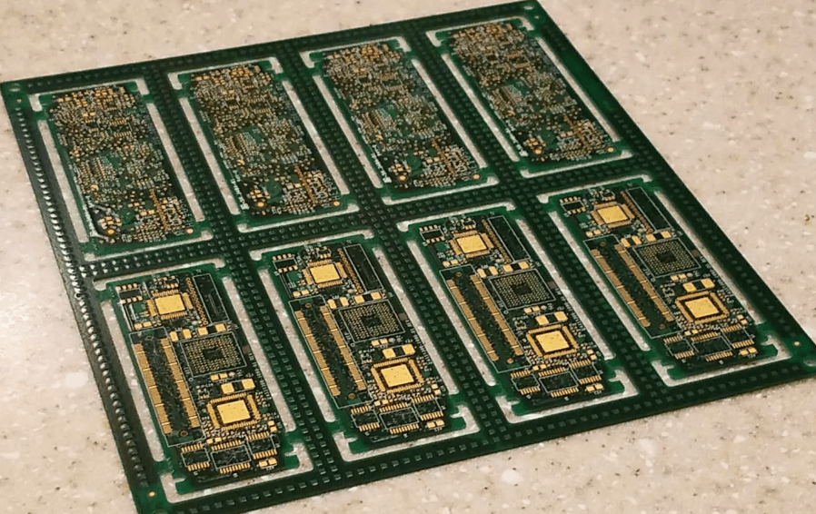
VII. Panel assembly: The finished surface is also a difficult aspect to fully consider during design:
When assembling panels, ease of machining is paramount. When milling the surface, the distance between the panel and the edge of the board should be consistent with the milling cutter diameter (typically 1.6, 1.2, 1.0, or 0.8 mm). When punching the surface, ensure that the distance between the holes and lines and the board edge is greater than one board thickness. The minimum punched slot size should be greater than 0.8mm. When using V-cut connections, the edge traces and copper foil must be kept 0.3mm from the center of the V-cut.
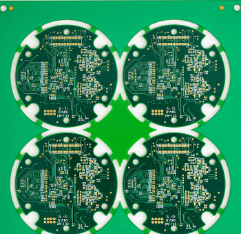
Secondly, consider the utilization of bulk material. Since bulk material specifications are relatively fixed, commonly used sheet metal sizes include 930×1245, 1040×1245, and 1090×1245. Improper panelization of the delivery unit can easily lead to material waste.