What rules should be followed when designing PCB pads?
1.PCB pads
PCB pads: Components are fixed to the PCB through the lead holes on the PCB with solder, and the printed wires connect the pads to achieve electrical connection of the components in the circuit. The lead holes and the surrounding copper foil are called pads.
Types of PCB pads include:
Square pads – often used when the components on the printed board are large and few, and the printed wires are simple. When making PCBs by hand, this type of pad is easy to implement. Round pads – widely used in single- and double-sided printed boards with regular arrangement of components. If the density of the board allows, the pads can be larger so that they will not fall off during welding.
Island pads – the connection between pads is integrated.
Often used in vertical irregular arrangement installations. For example, this type of pad is often used in tape recorders.
Teardrop pads – often used when the traces connected to the pads are thin to prevent the pads from peeling and the traces from the pads from being disconnected. This type of pad is often used in high-frequency circuits.
Polygonal pads – used to distinguish pads with similar outer diameters but different hole diameters, which is convenient for processing and assembly.
Oval pads – This type of pad has enough area to enhance anti-peeling ability and is often used for dual in-line devices.
Open pads – commonly used to ensure that the pad holes of manual soldering are not sealed by solder after wave soldering.
2.What rules should be followed when designing PCB pads?
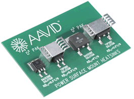
PCB pad design guide First, let’s define exactly what a “pad” is. A pad (also called a “pad”) is an exposed area of metal on a circuit board to which the leads of a part will be soldered. Multiple pads are used to create a component footprint or pad pattern on a printed circuit board.
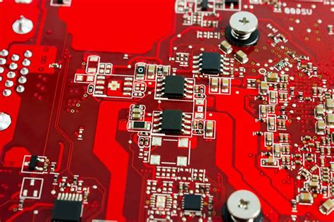
For through-hole components, the pad is usually circular and will have a plated hole through it so that the component lead can be inserted and soldered. For surface mount technology (SMT) parts, the size and shape of the pad will vary, depending on the component to be soldered. Sometimes, irregularly sized, shaped pads are used for thermal or mechanical reasons, while small circular pads are often used for alignment and registration with automated optical equipment.
Years after the introduction of PCB design tools, layout engineers had to manually define their own pads due to the lack of automated tools. This was done by drawing the pad shape in the design tool using information from the datasheet and general pad size and shape formulas.

However, this process can be prone to error because manufacturers’ specifications do not always follow the same formulas.
This can cause layout designers to use the wrong size and shape in their pads. Unfortunately, these incorrect pad sizes and shapes can have disastrous consequences during manufacturing, including:
· Via breakout: Via pads must have a solid annular ring for soldering, which is the metal between the hole wall and the periphery of the pad. The annular ring specification is designed to be large enough to allow for the expected amount of drill drift from the center of the hole. However, if the pad is too small, the annular ring may break, and too much breakage can result in improper soldering or a broken and incomplete circuit.
· Inadequate solder joints: SMT parts with too small pads may run the risk of not getting the right solder fillet during manufacturing. Without good fillet, solder joints will be weak and can crack.
· Floating parts: SMT parts that are soldered to pads that are too large can end up floating out of place during reflow. This can cause conflicts with other parts or even shorts between circuits.
· Logged-out parts: Two smaller SMT fixed-pin parts can have soldering issues if they have pads of different sizes, such as resistors and capacitors. One pad will heat up faster than the other, and the molten solder will pull the parts up and away from the other pad, sticking to it like a tombstone.
· Shorts to other metals: Pads that are too small can cause surface traces to get too close to the parts they are soldered to, potentially causing areas where metals short together. On the other hand, pads that are too large can restrict the routing of traces between them, making it more difficult to route the board.
All of these issues force PCB manufacturers to resort to hand-assembly techniques to solve these problems, while also spending more time on inspection and rework. Creating properly sized and shaped PCB pads is critical, and thankfully, there is a lot of help available today.