When to use thermal relief pcb
Importance Of Thermal Relief In High-Power PCB Designs
In high-power PCB designs, the importance of thermal relief cannot be overstated. As electronic devices become more powerful and compact, managing heat dissipation effectively is crucial to ensure the reliability and longevity of the components.
Thermal relief, a technique used in PCB design, plays a pivotal role in achieving this goal.
It involves creating a thermal pathway that allows heat to be conducted away from heat-generating components, thereby preventing overheating and potential damage.
One of the primary reasons for using thermal relief in high-power PCB designs is to maintain the integrity of solder joints.
When a component is soldered to a PCB, the heat from the soldering process can cause thermal stress. Without proper thermal relief, this stress can lead to weak or cracked solder joints, which can compromise the electrical connection and lead to device failure. By incorporating thermal relief, designers can ensure that the heat is distributed more evenly, reducing the risk of thermal stress and enhancing the durability of the solder joints.
Moreover, thermal relief is essential for maintaining the performance of high-power components.
Components such as power transistors, voltage regulators, and high-current connectors generate significant amounts of heat during operation. If this heat is not effectively dissipated, it can lead to thermal runaway, where the component’s temperature continues to rise uncontrollably, potentially causing permanent damage. Thermal relief helps to mitigate this risk by providing a controlled pathway for heat to escape, thereby maintaining the component’s temperature within safe operating limits.
In addition to protecting individual components, thermal relief also contributes to the overall thermal management of the PCB.
High-power designs often involve multiple heat-generating components placed in close proximity. Without adequate thermal relief, the cumulative heat generated by these components can create hotspots on the PCB, leading to uneven temperature distribution and potential thermal failure. By strategically implementing thermal relief, designers can ensure a more uniform temperature distribution across the PCB, enhancing the overall thermal performance and reliability of the design.
Furthermore, thermal relief can improve the manufacturability of high-power PCBs.
During the PCB fabrication process, thermal relief can help to prevent issues such as warping and delamination, which can occur due to uneven heating and cooling. By providing a controlled thermal pathway, thermal relief helps to minimize these manufacturing defects, resulting in higher quality and more reliable PCBs.
It is also worth noting that thermal relief can aid in the testing and troubleshooting of high-power PCBs.
When diagnosing thermal issues, having a well-designed thermal relief structure can make it easier to identify and address problem areas. This can save valuable time and resources during the testing phase, ensuring that any thermal issues are resolved before the PCB is deployed in the final product.
In conclusion, the importance of thermal relief in high-power PCB designs cannot be overlooked. It plays a critical role in maintaining the integrity of solder joints, protecting high-power components, ensuring overall thermal management, improving manufacturability, and aiding in testing and troubleshooting. As electronic devices continue to evolve, the need for effective thermal management solutions will only become more pronounced. By incorporating thermal relief into their designs, engineers can ensure that their high-power PCBs are capable of meeting the demanding thermal requirements of modern electronic applications.
Thermal Relief Strategies For Multi-Layer PCBs
Thermal relief strategies for multi-layer PCBs are crucial for ensuring the reliability and performance of electronic devices. When designing multi-layer printed circuit boards (PCBs), engineers must consider various factors, including thermal management, to prevent overheating and ensure efficient operation. One effective method for managing heat dissipation in multi-layer PCBs is the use of thermal reliefs. Understanding when to use thermal reliefs can significantly impact the overall functionality and longevity of the PCB.
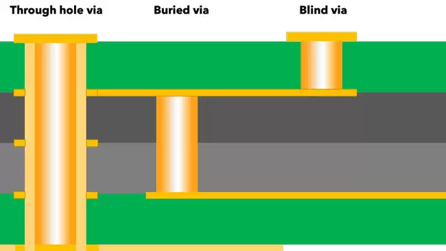
Thermal reliefs are essentially small, thermally conductive pathways that connect a pad to a larger copper plane.
These pathways are designed to balance the need for electrical connectivity with the need to manage heat dissipation. In multi-layer PCBs, thermal reliefs are particularly important because they help mitigate the thermal stress that can occur during soldering and operation. Without proper thermal reliefs, the heat generated during these processes can cause warping, delamination, or even complete failure of the PCB.
One of the primary scenarios in which thermal reliefs should be used is during the soldering process.
When a PCB is subjected to high temperatures during soldering, the heat can cause significant thermal expansion. If a pad is directly connected to a large copper plane without a thermal relief, the heat will dissipate unevenly, leading to potential soldering defects such as cold joints or insufficient solder flow. By incorporating thermal reliefs, the heat is distributed more evenly, allowing for a more controlled and reliable soldering process.
Another critical situation where thermal reliefs are beneficial is in high-power applications.
Multi-layer PCBs used in power electronics, such as power supplies or motor controllers, often handle substantial amounts of current. The high current flow generates considerable heat, which must be effectively managed to prevent damage to the PCB and its components. Thermal reliefs help to dissipate this heat more efficiently by providing a controlled thermal pathway, reducing the risk of overheating and ensuring the stability of the PCB.
Moreover, thermal reliefs are essential in applications where precise temperature control is required.
For instance, in sensitive electronic devices such as medical equipment or aerospace systems, maintaining a stable operating temperature is critical. Thermal reliefs aid in achieving this stability by preventing localized hotspots and ensuring uniform heat distribution across the PCB. This uniformity is vital for the accurate functioning of temperature-sensitive components and the overall reliability of the device.
In addition to these scenarios, thermal reliefs are also advantageous in multi-layer PCBs with high component density.
As the number of components on a PCB increases, so does the complexity of heat management. Thermal reliefs help to alleviate this complexity by providing a structured approach to heat dissipation. They allow for better thermal regulation, reducing the likelihood of thermal-induced failures and enhancing the overall performance of the PCB.
In conclusion, the use of thermal reliefs in multi-layer PCBs is a critical strategy for effective thermal management. By incorporating thermal reliefs, engineers can ensure more reliable soldering processes, manage high-power applications, maintain precise temperature control, and handle high component densities. Understanding when and how to use thermal reliefs can significantly enhance the performance and longevity of multi-layer PCBs, ultimately leading to more reliable and efficient electronic devices.
When To Use Thermal Relief In High-Density PCB Layouts
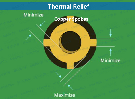
In high-density PCB layouts, the decision to use thermal relief is crucial for ensuring both the manufacturability and reliability of the final product. Thermal relief refers to the practice of connecting a pad to a plane with a series of narrow traces, rather than a solid connection. This technique is particularly important in high-density designs where numerous components are packed into a limited space, leading to potential thermal management challenges.
One of the primary reasons to use thermal relief in high-density PCB layouts is to facilitate the soldering process.
During soldering, components are subjected to high temperatures, and a direct connection to a large copper plane can cause uneven heating. This uneven heating can result in poor solder joints, as the heat is quickly dissipated into the plane, making it difficult to achieve the necessary temperature for proper solder flow. By using thermal relief, the heat is more evenly distributed, allowing for more consistent and reliable solder joints.
Moreover, thermal relief is essential for preventing thermal stress on the PCB.
In high-density layouts, the proximity of components can lead to localized hotspots, which can cause thermal expansion and contraction. This thermal cycling can induce mechanical stress on the solder joints and the PCB material itself, potentially leading to cracks and failures over time. Thermal relief helps to mitigate these effects by providing a controlled path for heat dissipation, thereby reducing the risk of thermal-induced damage.
In addition to soldering and thermal stress considerations, thermal relief also plays a role in electrical performance.
High-density PCBs often involve complex signal routing and power distribution networks. Direct connections to large copper planes can introduce parasitic inductance and capacitance, which can adversely affect signal integrity and power delivery. Thermal relief structures help to minimize these parasitic effects by providing a more controlled impedance path, thereby enhancing the overall electrical performance of the PCB.
Furthermore, thermal relief is beneficial for manufacturability, particularly in the context of rework and repair.
High-density PCBs are more prone to defects due to the close spacing of components and traces. When rework is necessary, such as replacing a faulty component, thermal relief makes it easier to apply localized heat without affecting adjacent areas. This localized heating capability is crucial for avoiding collateral damage during rework, ensuring that the integrity of the surrounding components and traces is maintained.
It is also important to consider the specific requirements of the application when deciding on the use of thermal relief.
For instance, in high-power applications where efficient heat dissipation is critical, the design may need to balance the benefits of thermal relief with the need for robust thermal management. In such cases, a hybrid approach may be employed, where thermal relief is used selectively to optimize both thermal and electrical performance.
In conclusion, the use of thermal relief in high-density PCB layouts is a multifaceted decision that impacts soldering quality, thermal management, electrical performance, and manufacturability. By carefully considering these factors, designers can ensure that their high-density PCBs are both reliable and efficient, meeting the stringent demands of modern electronic applications. The strategic implementation of thermal relief structures is thus a key aspect of successful high-density PCB design, contributing to the overall performance and longevity of the final product.
Benefits Of Thermal Relief In Preventing PCB Overheating
Thermal relief in printed circuit boards (PCBs) is a crucial design consideration that can significantly impact the performance and longevity of electronic devices.
One of the primary benefits of incorporating thermal relief in PCB design is its ability to prevent overheating, which can lead to a myriad of issues, including component failure, reduced efficiency, and even catastrophic damage to the entire system. Understanding when to use thermal relief in PCB design is essential for engineers and designers aiming to optimize the thermal management of their electronic products.
To begin with, thermal relief is particularly beneficial in high-power applications where components generate substantial amounts of heat.
In such scenarios, the risk of overheating is elevated, and without adequate thermal management, the heat can accumulate, causing the temperature of the PCB to rise to dangerous levels. By incorporating thermal relief, designers can ensure that heat is efficiently dissipated away from critical components, thereby maintaining a stable operating temperature and preventing thermal-induced failures.
Moreover, thermal relief is advantageous in densely populated PCBs where space constraints make it challenging to implement traditional cooling methods such as heat sinks or fans.
In these compact designs, thermal relief can be integrated into the PCB layout to facilitate heat dissipation without occupying additional space. This is achieved by creating thermal vias or using copper pours that connect heat-generating components to larger thermal masses, such as ground planes or heat spreaders. Consequently, the heat is distributed more evenly across the PCB, reducing hotspots and enhancing overall thermal performance.
In addition to high-power and densely populated applications, thermal relief is also essential in PCBs that operate in harsh environmental conditions.
For instance, electronic devices used in automotive, aerospace, or industrial settings are often exposed to extreme temperatures and fluctuating thermal loads. In such environments, the reliability of the PCB is paramount, and thermal relief can play a critical role in ensuring that the board can withstand these demanding conditions. By providing a pathway for heat to escape, thermal relief helps to maintain the integrity of the PCB and its components, thereby extending the lifespan of the device.
Furthermore, thermal relief is beneficial in improving the manufacturability of PCBs.
During the soldering process, uneven heat distribution can lead to issues such as solder bridging, cold joints, or component misalignment. By incorporating thermal relief, designers can create a more uniform thermal profile, which facilitates better solder flow and adhesion. This not only enhances the quality of the solder joints but also reduces the likelihood of defects, leading to higher yields and more reliable end products.
It is also worth noting that thermal relief can contribute to the overall efficiency of electronic devices.
By maintaining optimal operating temperatures, thermal relief helps to ensure that components function within their specified thermal limits, thereby maximizing their performance and energy efficiency. This is particularly important in applications where power consumption is a critical factor, such as in portable or battery-operated devices. By preventing overheating, thermal relief can help to minimize power losses and extend battery life, resulting in more efficient and sustainable electronic products.
In conclusion, the benefits of thermal relief in preventing PCB overheating are manifold. From enhancing thermal management in high-power and densely populated designs to improving reliability in harsh environments and manufacturability, thermal relief is an indispensable tool for PCB designers. By understanding when and how to use thermal relief, engineers can optimize the performance, reliability, and efficiency of their electronic devices, ensuring that they meet the demands of modern applications.