Why Are PCB Layers Mostly Even-Numbered?
Introduction
Printed Circuit Board (PCB) design represents one of the most fundamental aspects of modern electronics manufacturing. Among the many design considerations that engineers must address, the decision regarding the number of layers in a PCB holds particular significance. A curious pattern emerges when examining multilayer PCBs across the industry: the overwhelming majority feature an even number of conductive layers. This phenomenon isn’t coincidental but rather stems from a combination of technical, economic, and manufacturing factors that make even-layer PCBs more practical and cost-effective in most applications.
This article will explore the multiple reasons behind this industry preference, examining the manufacturing processes, material considerations, structural integrity aspects, cost factors, and performance characteristics that collectively make even-numbered layer counts the dominant choice in PCB design. We’ll also consider the exceptional circumstances where odd-layer PCBs might be used and how modern manufacturing techniques are evolving to potentially change this long-standing practice.
Manufacturing Process Considerations
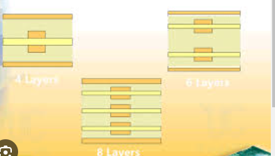
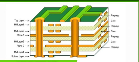
Core and Prepreg Stackup
The manufacturing process for multilayer PCBs fundamentally relies on alternating layers of conductive copper and insulating dielectric material. The industry-standard approach builds boards around a central core—a basic double-sided PCB consisting of copper layers bonded to both sides of a dielectric substrate. Additional layers are then added using prepreg (pre-impregnated) dielectric material and copper foil.
This core-based construction naturally leads to even-numbered layer counts because:
- Every core provides two conductive layers
- Additional layers are always added in pairs (one on each side) to maintain symmetry
- The lamination process works most effectively with balanced, symmetrical layer stacks
Lamination Symmetry Requirements
PCB lamination—the process of bonding multiple layers under heat and pressure—requires careful attention to symmetry to prevent warping and other structural issues. When layers are added asymmetrically (as would be required for an odd-layer count), the differing thermal expansion characteristics and material stresses often lead to manufacturing defects.
The symmetrical stackup of even-layer PCBs provides:
- Balanced thermal mass distribution during lamination
- Uniform curing of prepreg materials
- Equal copper distribution across the board’s Z-axis
- Reduced mechanical stress during cooling
Copper Plating and Patterning
The plating processes used to create conductive vias and through-holes work most effectively with even layer counts. The electroplating bath requires uniform current distribution, which is more easily achieved with symmetrical layer arrangements. Additionally, photolithographic patterning processes benefit from the consistent material properties of balanced layer stacks.
Structural Integrity and Reliability
Warpage Prevention
One of the most critical reasons for preferring even-layer counts relates to preventing PCB warpage—a deformation that can cause significant reliability issues in assembled electronics. The different coefficients of thermal expansion between copper and dielectric materials mean that asymmetric layer stacks tend to warp during manufacturing processes and subsequent thermal cycling.
Even-layer PCBs provide:
- Balanced copper distribution above and below the neutral axis
- Symmetrical thermal expansion forces
- Reduced bending moments during temperature changes
- Better flatness for surface mount assembly processes
Mechanical Stress Distribution
The mechanical stresses experienced by a PCB during manufacturing, assembly, and operation distribute more evenly in symmetrical, even-layer constructions. This balanced stress distribution leads to:
- Reduced risk of delamination between layers
- Improved via reliability (particularly for through-hole vias)
- Better performance under mechanical shock and vibration
- Enhanced long-term reliability in harsh environments
Layer Registration and Alignment
Maintaining precise alignment between layers becomes increasingly challenging with higher layer counts. Even-layer PCBs benefit from:
- Symmetrical registration targets
- Balanced optical alignment systems
- Uniform pressure distribution during lamination
- More consistent drilling conditions for vias
Cost and Production Efficiency Factors
Material Utilization
PCB fabrication makes most efficient use of materials with even layer counts. The standard manufacturing approach uses panel sizes that accommodate pairs of layers most economically. Odd-layer designs often require:
- Additional processing steps
- Specialized lamination sequences
- Higher material waste
- More complex inventory management
Processing Time and Yield
Even-layer PCBs typically show:
- Higher production yields
- Fewer lamination defects
- More consistent electrical testing results
- Faster processing times
- Better compatibility with automated inspection systems
These factors directly translate to lower manufacturing costs per unit, making even-layer designs more economically attractive for most applications.
Standardization Benefits
The PCB industry has developed around even-layer constructions, leading to:
- Widely available even-layer materials
- Optimized equipment configurations
- Established design rules and guidelines
- Predictable performance characteristics
- Simplified supply chain logistics
This standardization creates a strong economic incentive to stay with even-layer designs unless odd-layer counts offer compelling advantages for specific applications.
Signal Integrity and Electrical Performance
Impedance Control
Modern high-speed digital designs require precise control over transmission line impedance. Even-layer PCBs provide:
- More consistent dielectric thicknesses
- Symmetrical reference planes
- Balanced coupling between adjacent layers
- Predictable cross-talk characteristics
Power Distribution
The power delivery network (PDN) in multilayer PCBs benefits from even-layer counts through:
- Symmetrical power/ground plane pairs
- Balanced decoupling capacitor placement
- Uniform current distribution
- Reduced simultaneous switching noise
EMI and Shielding
Electromagnetic interference (EMI) control improves with even-layer designs because:
- Shielding layers can be symmetrically placed
- Current return paths remain balanced
- Ground plane interruptions are minimized
- Edge radiation patterns are more predictable
When Odd-Layer PCBs Are Used
Despite the overwhelming preference for even layers, certain situations may justify odd-layer PCB designs:
Cost Reduction in Simple Designs
Very low-cost products might use single-layer or 3-layer designs when:
- Circuit complexity is minimal
- Signal integrity requirements are relaxed
- Board space constraints aren’t severe
- Component density is low
Specialized Applications
Some RF/microwave designs or unusual form factors might require odd layers to:
- Achieve specific dielectric thicknesses
- Accommodate unique component placements
- Meet mechanical constraints
- Optimize thermal paths
Advanced Manufacturing Techniques
Emerging technologies like sequential lamination and embedded components are making odd-layer designs more practical by:
- Allowing asymmetric layer additions
- Incorporating passive components within layers
- Using advanced materials with different properties
- Enabling 3D interconnection structures
The Future of PCB Layer Counts
As manufacturing technologies evolve, some traditional constraints favoring even-layer counts may diminish:
Advanced Materials
New dielectric materials with:
- Lower thermal expansion coefficients
- Improved dimensional stability
- Enhanced mechanical properties
may reduce the warpage risks associated with odd-layer designs.
Manufacturing Innovations
Process improvements like:
- Laser direct imaging
- Automated optical alignment
- Precision lamination control
- Additive manufacturing techniques
could make odd-layer PCBs more practical and cost-effective.
Design Tool Advancements
Modern EDA tools with:
- 3D electromagnetic simulation
- Advanced thermal modeling
- Mechanical stress analysis
- AI-driven optimization
may help designers successfully implement odd-layer designs when appropriate.

Conclusion
The predominance of even-layer PCBs in the electronics industry stems from a convergence of manufacturing realities, material properties, reliability requirements, and economic factors. The symmetrical construction of even-layer boards provides inherent advantages in warpage control, structural integrity, production yield, and electrical performance that have made them the default choice for most applications.
While odd-layer PCBs remain viable for specific use cases, the comprehensive benefits of even-layer designs ensure their continued dominance in PCB technology. As manufacturing capabilities advance, we may see more frequent use of odd-layer counts in specialized applications, but the fundamental advantages of symmetry in multilayer construction suggest that even-layer PCBs will remain the standard approach for the foreseeable future.
Understanding these layer count considerations helps designers make informed decisions when planning PCB architectures, balancing technical requirements with manufacturing practicality to create optimal solutions for each electronic product’s needs.