Why Do PCB Boards Warp and How to Determine If a PCB Is Warped?
Introduction
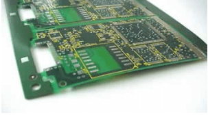
Printed Circuit Boards (PCBs) are fundamental components in modern electronics, serving as the backbone for mounting and interconnecting electronic components. However, one of the most common issues affecting PCB quality and reliability is board warping or deformation. PCB warpage can lead to significant problems during assembly, soldering, and final product operation. This article explores the root causes of PCB warping and provides comprehensive methods to detect and measure PCB deformation.
Causes of PCB Warping
1. Material Selection and Properties
The base materials used in PCB fabrication play a crucial role in determining the board’s susceptibility to warping:
- CTE Mismatch: Different materials have varying Coefficients of Thermal Expansion (CTE). When materials with different CTEs are combined in a multilayer PCB, they expand and contract at different rates during temperature changes, leading to stress and potential warping.
- Material Quality: Low-quality substrate materials or inconsistent material properties can lead to uneven stress distribution, making the board more prone to warping.
- Glass Transition Temperature (Tg): Materials with lower Tg values are more likely to deform when exposed to high temperatures during manufacturing processes.
2. Manufacturing Processes
Several manufacturing steps can introduce stresses that lead to PCB deformation:
- Lamination Process: Improper lamination pressure, temperature, or time can result in incomplete bonding or residual stresses between layers.
- Copper Distribution: Uneven copper distribution across PCB layers creates unbalanced stresses. Areas with dense copper patterns expand differently from areas with sparse copper.
- Cooling Rates: Rapid cooling after high-temperature processes can lock in thermal stresses, leading to warping as the board returns to room temperature.
3. Design Factors
PCB design choices significantly impact warpage potential:
- Asymmetric Layer Stackup: Non-symmetrical arrangement of copper layers or dielectric materials creates imbalanced stresses.
- Uneven Copper Thickness: Variations in copper thickness across layers lead to different contraction rates during cooling.
- Large Size and Thin Boards: Larger and thinner PCBs are more susceptible to warping due to reduced structural rigidity.
4. Environmental Factors
External conditions can contribute to PCB deformation:
- Moisture Absorption: Many PCB materials are hygroscopic and can absorb moisture, leading to expansion and potential warping.
- Thermal Cycling: Repeated exposure to temperature variations in operation can cause cumulative warpage over time.
- Mechanical Stress: Physical bending or twisting during handling, assembly, or use can induce permanent deformation.

Methods to Determine PCB Warping
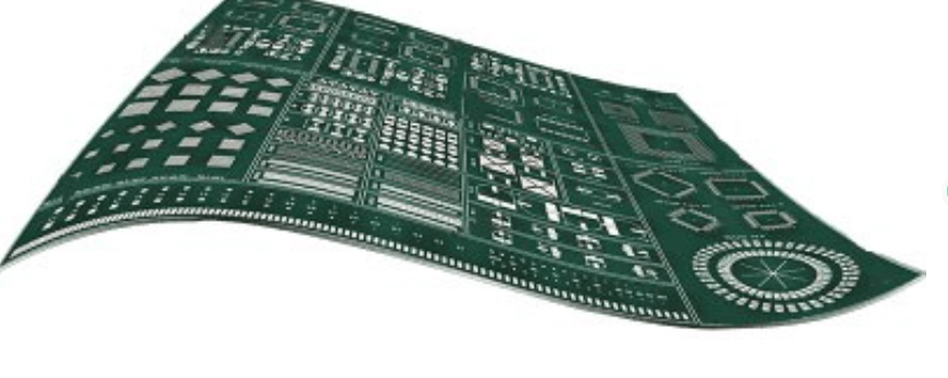
1. Visual Inspection
The simplest method involves visual assessment:
- Lay Flat Test: Place the PCB on a perfectly flat surface and check for gaps between the board and surface.
- Edge Observation: View the board from the side to observe any visible curvature or twisting.
- Shadow Method: Shine a light from one side and observe the shadow pattern for irregularities.
2. Mechanical Measurement Tools
Precise warpage measurement requires specialized tools:
- Height Gauge: Measure the height of board corners relative to a flat surface.
- Dial Indicator: Use a precision dial gauge to measure vertical displacement at multiple points.
- Coordinate Measuring Machine (CMM): For high-precision applications, CMMs can map the entire board surface topography.
3. Optical Measurement Systems
Advanced non-contact methods provide accurate warpage data:
- Laser Scanning: Laser displacement sensors can quickly scan the PCB surface to create a 3D profile.
- Moire Projection: Projects a pattern onto the PCB surface and analyzes the distortion to calculate warpage.
- Digital Image Correlation: Uses camera systems to track surface deformation under different conditions.
4. IPC Standards for Warpage Measurement
The IPC (Association Connecting Electronics Industries) provides standardized methods:
- IPC-TM-650 2.4.22: Standard test method for bow and twist of printed boards.
- IPC-6012: Qualification and performance specification for rigid PCBs, including warpage limits.
- Acceptance Criteria: Typically, warpage should not exceed 0.75% for SMT assemblies (e.g., 0.75mm for a 100mm board).
5. Warpage Measurement During Reflow
Specialized techniques for assessing warpage under thermal conditions:
- Shadow Moire: Measures real-time warpage changes during temperature profiles simulating reflow.
- Thermal Mechanical Analysis (TMA): Tracks dimensional changes versus temperature.
- In-line Inspection Systems: Automated optical inspection (AOI) systems with warpage measurement capabilities.
Preventing PCB Warping
Understanding the causes of warping leads to effective prevention strategies:
1. Design Considerations
- Maintain symmetrical layer stackup with balanced copper distribution
- Use similar materials with compatible CTEs in multilayer boards
- Avoid large copper-free areas that create imbalance
- Consider thicker cores for large boards
2. Material Selection
- Choose high-quality base materials with appropriate Tg
- Select materials with low moisture absorption rates
- Consider using stiffener materials for flexible applications
3. Manufacturing Controls
- Optimize lamination parameters (pressure, temperature, time)
- Implement controlled cooling processes
- Ensure proper storage conditions to prevent moisture absorption
- Use panelization techniques that minimize stress
4. Process Verification
- Implement warpage measurement at critical process steps
- Conduct pre-assembly flatness checks
- Perform thermal cycling tests to assess long-term stability
Conclusion
PCB warping is a complex issue resulting from material properties, design choices, manufacturing processes, and environmental factors. Understanding these causes enables better prevention strategies throughout the product lifecycle. Accurate warpage detection requires appropriate measurement techniques ranging from simple visual checks to advanced optical systems, with IPC standards providing guidance for acceptable limits.
By implementing proper design practices, material selection, manufacturing controls, and thorough inspection protocols, manufacturers can significantly reduce PCB warping issues. This leads to improved production yields, better solder joint reliability, and enhanced long-term performance of electronic assemblies.
As electronic devices continue to evolve with more complex PCBs operating in demanding environments, warpage control remains a critical factor in ensuring product quality and reliability. Ongoing advancements in materials science, manufacturing technologies, and inspection methods will continue to address the challenges of PCB deformation in the electronics industry.