Why do PCBs need to be assembled? What are the techniques for PCB assembly?
PCBs have many functions and features in electronic devices. High density, high reliability, designability, etc. are all characteristics of PCBs. In order to enhance everyone’s understanding of PCBs, this article will introduce why PCBs need to be assembled and explain the techniques for PCB assembly. If you are interested in PCBs, you may wish to continue reading.
1.Why do PCBs need to be assembled?
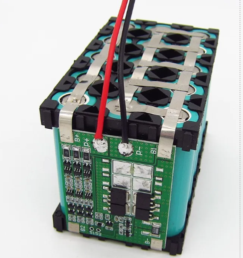
PCB (printed circuit board) is a printed circuit board, or printed circuit board for short, which is one of the important components of the electronics industry. Almost every electronic device, from electronic watches and calculators to computers, communication electronic equipment, and military weapon systems, as long as there are electronic components such as integrated circuits, in order to make electrical interconnections between the components, printed boards must be used.
The printed circuit board consists of an insulating base plate, connecting wires, and pads for assembling and welding electronic components. It has the dual functions of a conductive line and an insulating base plate. It can replace complex wiring and realize the electrical connection between components in the circuit. It not only simplifies the assembly and welding of electronic products, reduces the wiring workload under traditional methods, and greatly reduces the labor intensity of workers; it also reduces the size of the whole machine, reduces product costs, and improves the quality and reliability of electronic equipment.
The printed circuit board has good product consistency. It can adopt standardized design, which is conducive to mechanization and automation in the production process. At the same time, the whole piece of assembled and debugged printed circuit board can be used as an independent spare part, which is convenient for the interchange and maintenance of the whole product. At present, printed circuit boards have been widely used in the production and manufacturing of electronic products.
So, why do PCBs often need to be plated?
1.PCB production size requirements
Generally speaking, we need to plate smaller boards. Generally, boards with a single side less than 50mm need to be plated. Because when the designed plate size is smaller than the machine’s production size, our machine cannot produce it, so we need to plate to meet the minimum size requirements of machine production. So what is the maximum size we can plate? Generally speaking, the maximum plate size should not exceed 700mm*600mm. Only when the size of our plate is controlled within this range can our patch efficiency be guaranteed.
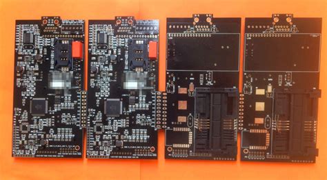
2.Avoid waste of PCB board
When the PCB board is special-shaped or there are multiple PCBs with the same process, we can also plate, which can save board, make full use of our resources and avoid board waste.
3.After understanding why we need to plate, let’s learn about the matters that we need to pay attention to when we plate.
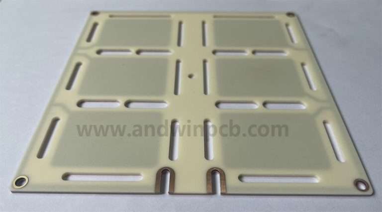
In order to facilitate our production, try to keep the plate in a square shape after plated. In short, don’t let the length and width ratio be too different.
We usually use v-cut to splice regular boards. V-cut cannot be used to splice special-shaped boards and frames, so we use stamp holes to splice special-shaped boards and frames.
For PCBs with components on the outermost side less than 3mm from the edge of the board, process edges must be added, usually with the longer side as the process edge; this is why we usually add process edges to single boards.
After splicing the board, don’t forget to add three mark points and place four non-metallized holes on the outer process edge. Note that the mark points at the diagonal corners should not be placed in a straight line, but slightly staggered.
A space of >0.5mm should be reserved between the components and the V-CUT to ensure the normal operation of the tool.
4.PCB splicing skills
PCB splicing is something that PCB factories often do. What matters need to be paid attention to when splicing? What are the key points of PCB splicing? Summarize it for you as follows:
First of all, the problem of splicing. We know that the main problem of splicing is to save production costs. For PCB splicing, the width is ≤260mm~300mm, which varies according to different production lines. Because we may have a lot of materials, and the processing equipment itself has one gun corresponding to one module, so if the panel exceeds the range of the module, the processing speed will become very slow.
The outer frame (clamping edge) of the PCB panel should be carefully considered to ensure that the PCB panel will not deform after being fixed on the fixture (generally, V-grooves are not allowed on this edge). For the layout of components, first, all directions must be consistent, and mirror images cannot appear, which will cause problems with the coordinate positioning of the processing.
Second, there should be no connector protruding from the edge (between the outer frame of the panel and the internal small board, and between small boards). If this happens, it will hinder the tool from separating the boards after welding is completed.
In order to ensure the position and level of the detection board, we need to set more than three positioning points on the edge of the board. By optically detecting these three points, the reference coordinates of the entire processing and the levelness of the board can be obtained.
The correct approach is to leave 5mm from the edge and the spacing is different when the direction of travel is inconsistent (to facilitate distinguishing the direction of entry): [When setting the reference positioning point, usually leave a non-resistance solder area 1.5 mm larger than it around the positioning point, and there should be no similar pads or other similar ones]
There must be at least three positioning holes on each small board, 3≤aperture≤6 mm, and wiring or patching is not allowed within 1mm of the edge positioning hole (to prevent misjudgment). PCB panelization is mainly to save production and processing costs (it will make the machine processing speed several times faster). Unreasonable design will make the later stage full of problems. You can take a closer look to prevent problems.
First of all, there is the problem of panelization. We know that the main problem of panelization is to save production costs. For PCB panelization width ≤260mm~300mm, it varies according to different production lines. Because we may have a lot of materials, and the processing equipment itself has one material gun corresponding to one module, so if the panelization exceeds the range of the module, the processing speed will become very slow.
The above is the content about PCB that the editor wants to share with you this time. I hope you have a certain understanding of the content shared this time. If you want to read articles of different categories, you can select the corresponding channel at the top of the webpage