Why Does PCB Design Software Show “No Connections” During DRC? Understanding and Resolving the Issue
Introduction
When working with Printed Circuit Board (PCB) design software, one of the most frustrating issues designers encounter is when the Design Rule Check (DRC) or connection verification tool reports “no connections” on what appears to be a properly routed board. This problem can halt your design workflow, delay projects, and potentially lead to manufacturing errors if not properly addressed. This article explores the various reasons why PCB software might display this misleading message and provides comprehensive solutions to resolve the issue.
Understanding the “No Connections” Error
The “no connections” warning typically appears during the DRC process when the software cannot detect electrical continuity between components that should be connected according to the schematic. This doesn’t necessarily mean there are no physical traces on the board—rather, it indicates that the software doesn’t recognize these traces as forming valid electrical connections.

Common Causes and Solutions
1. Netlist Mismatch Between Schematic and PCB
Problem: The most frequent cause of “no connections” errors is a discrepancy between the schematic netlist and the PCB layout. If you’ve made changes to the schematic without properly updating the PCB, or vice versa, the software may report missing connections.
Solution:
- Always synchronize your schematic and PCB after making changes
- Use the “Update PCB” or “Import Changes” feature in your EDA tool
- Verify that component designators match between schematic and PCB
- Check for unresolved differences in the Engineering Change Order (ECO) dialog
2. Incorrect Net Assignment
Problem: Traces might exist physically but aren’t assigned to the correct nets, causing the software to see them as unconnected.
Solution:
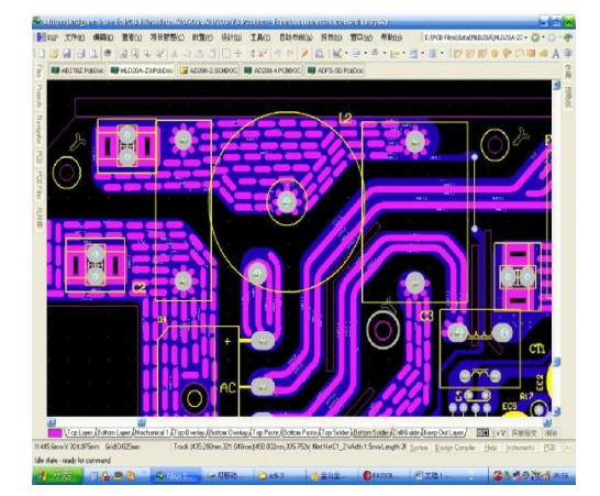
- Use the “Show Nets” feature to visualize net assignments
- Manually assign nets to traces if necessary
- Verify that net names match between schematic and layout
3. Connection Issues in the Schematic
Problem: The schematic itself might have connection problems that propagate to the PCB.
Solution:
- Run Electrical Rule Check (ERC) on the schematic first
- Look for these common schematic issues:
- Wires that appear connected but aren’t (missing junction dots)
- Components not properly wired (floating pins)
- Off-grid components causing visual but not electrical connections
- Hidden power pins not properly connected
4. Layer Configuration Problems
Problem: Connections might exist but aren’t recognized due to layer configuration issues.
Solution:
- Verify that all required layers are enabled
- Check layer pairing for proper via connections
- Ensure plane layers are properly defined and connected
- Confirm that the correct layer stackup is defined
5. Design Rule Constraints
Problem: Overly restrictive design rules might cause valid connections to be flagged as errors.
Solution:
- Review your DRC settings and constraints
- Adjust clearance rules if necessary
- Check minimum trace width requirements
- Verify via size and pad size rules
6. Component Footprint Issues
Problem: Incorrect or mismatched footprints can lead to connection problems.
Solution:
- Verify that pin numbers in the schematic symbol match pad numbers in the footprint
- Check for flipped or mirrored components
- Ensure all necessary pads exist in the footprint
- Confirm footprint land patterns match component specifications
7. Software Bugs or Glitches
Problem: Occasionally, the issue might stem from software bugs or file corruption.
Solution:
- Save and restart the design software
- Try opening the project on a different computer
- Export and re-import the design
- Check for software updates or patches
- Contact the software vendor’s support if the problem persists
Advanced Troubleshooting Techniques
When basic solutions don’t resolve the “no connections” issue, try these advanced techniques:
1. Net Comparison Analysis
Use your EDA tool’s net comparison feature to identify specific differences between the schematic netlist and PCB connections. This can pinpoint exactly where discrepancies occur.
2. Connectivity Verification Tools
Many PCB packages offer specialized connectivity verification tools that go beyond basic DRC. These can provide more detailed information about connection problems.
3. Manual Net Assignment
For critical connections, you might need to manually assign nets to traces or pads to force the correct connectivity.
4. Design For Manufacturability (DFM) Checks
Run DFM checks which often include more rigorous connectivity analysis that might reveal subtle issues standard DRC misses.
5. Export/Import Verification
Export your design to a neutral format (like ODB++) and re-import it to see if connectivity issues persist—this can help identify file corruption problems.

Prevention Best Practices
To avoid “no connections” errors in future projects:
- Maintain Synchronization: Always keep schematic and PCB in sync
- Follow Consistent Naming Conventions: Use clear, consistent net naming
- Implement Version Control: Use version control to track changes
- Document Design Rules: Clearly document and share design rules with your team
- Validate Libraries: Regularly verify component libraries for accuracy
- Use Hierarchical Design: For complex projects, hierarchical design can prevent connectivity issues
- Perform Regular Intermediate Checks: Don’t wait until final DRC to check connections
When to Seek Professional Help
If you’ve exhausted all troubleshooting steps and still face persistent “no connections” errors, consider:
- Contacting your EDA software’s technical support
- Consulting with experienced PCB designers
- Hiring a design service review for complex boards
- Attending advanced training for your specific EDA tool
Conclusion
The “no connections” error in PCB design software can stem from various causes ranging from simple synchronization issues to complex netlist discrepancies. By systematically checking schematic connections, verifying net assignments, ensuring proper layer configurations, and maintaining synchronization between schematic and layout, most connectivity issues can be resolved. Understanding your EDA tool’s specific behaviors and implementing robust design practices will minimize these problems in future projects. Remember that thorough verification at each design stage is far more efficient than trying to debug connectivity issues in a completed layout.
PCB design is as much an art as it is a science, and connection verification is one of its most critical aspects. By mastering the techniques outlined in this article, you’ll spend less time debugging false errors and more time creating reliable, manufacturable circuit boards.