Why does your pcb keep having solder pick-off?An Ultimate guide to Eliminating Hidden Dangers
In the world of electronics manufacturing,PCB soldering quality is the cornerstone of product reliability.However,experienced engineers and hobbyists alike have all experienced the problem of solder pick-off at some point.Watching supposedly smooth,plump solder joints become dry,rough,or even completely untinned leads is a deeply frustrating experience.
Poor solder pick-off essentially means that the molten solder fail to form a good,continuous,and smooth metallic bond with the PCB pad or component pin,This not only affects electrical connection performance but also poses a potential quality risk.To thoroughly resolve this issue,we must act like detectives,conducting a systematic investigation across multiple dimensions,including materials processes,design,and management.
This article will deeply analyze the six core causes of solder pick-off and provide practical solutions.
1:PCB Quality and Qxidation
The PCB is the foundation of soldering;a weak foundation can lead to shaky foundations.
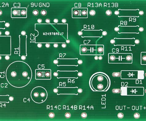
1.Pad Oxidation:This is one of the most common causes.PCB pads typically have an anti-oxidation coating applied to the copper surface.The most common coating are HASL(lead-free tin-spray galvannealing),ENIG(electroless immersion gold),and OSP(organic solder paste).
HASL:If stored for extended period(over3-6 months) or in high-temperature,high-humidity environments,the tin surface can oxidize,forming a dense oxide layer that hinders soldering.
ENIG:While the gold layer offers excellent oxidation resistance,the underlying nickel layer is susceptible to phosphorus content or contamination,forming a “black pad”that can lead to brittle fracture and poor solder penetration.
OSP:The protective film is extremely thin and cannot withstand repeated heating or prolonged storage.Once it wears off,the copper foil rapidly oxidizes.
2.Pad Contamination:During production or transportation,the pads can come into contact with sweat,oil dust,or other chemicals ,forming an insulating layer.
Solution:
Standardized Material Magememt.Treat PCBs as sensitive ,materials,sealing them,protecting them from light,and storing them in a constant temperature and humidity environment(recommended 25±5°C, humidity <60%), following the “first-in, first-out” principle.
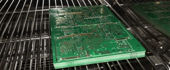
Pre-use Baking: For PCBs suspected of being damp or stored for an extended period, baking them before soldering (e.g., at 125°C for 2-4 hours) can effectively remove moisture and activate the pads.
Choose a Reliable Supplier:Partner with a reputable PCB manufacture to ensure their surface treatment is stable and reliable.

Culprit 2:Solder Paste Quality and Application Process
Solder paste is the “blood and blood”of soldering,and its condition directly determines soldering success.
1.Solder paste Oxidation/Deterioration:If solder paste is not used up within the specified timeframe after opening,or if is exposed to air for extended periods during use,the flux in it will deteriorate and the metal powder will oxidize
2.Improper Rewarming/Stirring:Inadequate rewarming(using directly from the refrigerator)can cause condensation,spattering,and oxidation,Inadequate stirring can cause the flux and metal powder to separate,affecting printing and soldering performance.
3.Inadequate Flux Activity:The selected solder paste’s flux activity level may not effectively remove the oxide
Solution:
Strictly Adhere to Solder Paste Usage Specifications:Strictly follow the datasheet instructions for rewarming(usually2-4 hours) and stirring(usually1-3 minutes),and use within the specified time after opening(usually within 24 hours).
Correct Solder paste Selection:Select a solder paste with appropriate activity based on product requirements and PCB conditions.For boards with slight oxidation,useRA(high activity)or RMA(medium activity),but be careful to clean any residue.
Manage the printing Environment:Control the temperature and humidity in the workshop and minimize the time the solder paste is exposed to the stencil.
Culprit 3:Hidden Dangers During the printing and Placement stages
This is a crucial step in accurately applying the “flesh and blood”to the “skeleton“
1.Stencil lssues
Improper opening Design:Insufficient opening area/width-to-thickness rations lead to poor solder paste release and insufficient solder application.
Opening Blockage/Contamination: Failure to promptly clean the stencil allows residual solder paste to dry and clog the openings.
Insufficient Tension:Stencil slackness leads to loose,uneven separation from the PCB during printing,resulting in a quiver or insufficient solder paste application.
2.Printer parameters:Improper setting for squeegee pressure,speed release distance, and speed can all affect solder paste buildup quality
3.Excessive Placement Pressure:Excessive pressure during component placement can squeeze solder paste out of the placement can squeeze solder applied.
Solution
Optimize stencil design:Collaborate with experienced engineers to design appropriate opening shapes and sizes based on component and pad characteristic.For fine-pitch component,utilize a laser cutting and electropolishing process.
Strictly perform daily printer maintenance:Regularly clean the stencil and check tension.
precisely set process parameters:Use a solder paste inspector(spi)to monitor and optimize printing parameters to ensure the solder paste volume,area,and height on each pad meet requirements.
Calibrate the placement machine:Ensure the placement head height and pressure are correctly set.
Culprit 4:Improper reflow profile
Reflow is the magical moment when”the Midas touch turns to gold”without the right profile,everything is in vain.
1.Excessive heating in the preheat/heating zone:This cause the flux to enter the high-temperature zone before it has fully evaporated,potentially causing solder scattering and premature flux deactivation.
2.Insufficient time or too low temperature in the constant temperature zone (activation zone): This is one of the most critical steps. If this stage is too short or the temperature is insufficient, the flux won’t have enough time to remove oxides from the pads and component leads, leading to poor soldering.
3.Insufficient peak temperature or too short a time in the reflow zone:The solder fails to fully melt and wet the pads,preventing the formation of a good intermetallic compound(IMC).
4.Impure nitrogen atmosphere:If a nitrogen furnace is used,excessive oxygen concentration can exacerbate oxidation.
Solution:
Accurately measure and optimize the reflow profile:Use an oven temperature tester to determine optimal oven temperature parameters based on the recommended solder paste profile and the actual product.Focus on the constant temperature zone settings.
Regularly maintain the reflow oven:Ensure uniform heating across all zones,proper fan operation,and that the nitrogen concentration meet specified standards.
Culprit 5:Problem with component lead/solder terminal
Sometime ,the problem isn’t with the PCB itself.
1.Component Oxidation:Especially for active device stored for long periods of time,the pin surface may oxidize.
2.Component Plating Issues:The component terminal plating (such as tin,silver,palladium,etc)is of poor quality or incompatible with the solder.
Solution
Incoming component inspection :For suspect batches,solderability testing can be performed.
Also follow the”first-in,first-out” principle to avoid storing components for extended periods.
Culprit six:PCB Design Defects
“Pitfalls”buried during the design phase are difficult to correct during manufacturing.
1.Direct connection of solder pads to GND or large copper areas:This causes heat to dissipate quickly during soldering ,preventing the actual pad temperature from reaching reflow requirements.This creates a “heat theft”phenomenon,leading to cold solder joints and poor soldering
2.Excessive or insufficient pad spacing :Excessive spacing can affect solder climbing due to capillary action;excessive spacing can cause bridging.
Solution:
Adopt a thermally isolated design:For solder pads that require soldering ,especially those connecting to large copper surfaces,use “thermal relief”to effectively reduce heat loss.
Follow DFM(Design for manufacturability)spcifications:Communication with process engineers during the layout phase to ensure the design meets production requirements.
Summary:Build a systematic defense system
Poor soldering is not caused by a single factor;It is a systemic problem.To address it a comprehensive quality defense system is needed from design-material procurement-storage-process setting -process monitoring.
Poor soldering is not caused by a single factor; it is a systemic problem. To address it, a comprehensive quality defense system is needed, from design -> material procurement -> storage -> process settings -> process monitoring.
If the problem recurs, we recommend troubleshooting the following steps:
- Macroscopic Observation: Is the soldering problem widespread or concentrated in specific areas/components?
- PCB Inspection: Observe the color and gloss of the pads, and use a magnifying glass to check for signs of oxidation.
- Process Review: Is the solder paste within its expiration date? Has the reflow profile changed recently? Is the stencil clean?
- In-depth Analysis: If necessary, use microscopy, SEM/EDS, or other tools to analyze the composition and structure of defective solder joints to pinpoint the root cause.
Remember, in electronics manufacturing, the devil is in the details. Only by maintaining meticulous attention to every step can you end the nightmare of poor soldering on your PCB, ensuring flawless solder joints and rock-solid products.