Why is it not recommended to use tin spraying process for high-speed PCB with crimped components?
Introduction to tin spraying process:
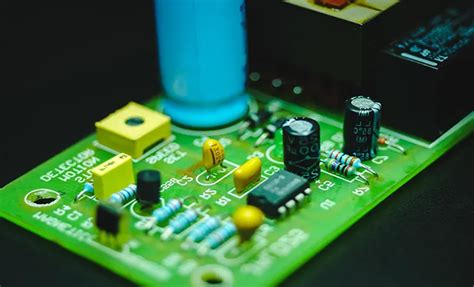
Tin spraying is also called hot air leveling. Through physical action, the printed circuit board is immersed in molten solder, and then the excess solder on the surface of the printed circuit board and in the metallized holes is blown off by hot air, thereby obtaining a smooth and bright solder coating layer.

The following figure shows the vertical tin spraying equipment commonly used in factories:
Advantages of tin spraying:
★ Mature process, mature industrial standards, high production speed
★ Reworkable, no whiskers, long storage time
★ Multiple assembly
Limitations of tin spraying:
★ Unable to meet small welding spacing, uneven thickness, and lead tin spraying is not environmentally friendly, and many products are not applicable
★ The thickness range of tin spraying is: 40-1000u” (micro inches)
★ The tin thickness range is relatively large, which can easily lead to uneven solder joint surface, or large changes in hole diameter, and even the undesirable phenomenon of tin spray blocking holes.
PCB factories usually give the following warnings when doing tin spraying process:
Hole less than 0.5mm has the risk of blocking holes, and the pressure holes of tin spraying plates have the risk of small holes, but most of our engineers do not have this risk awareness.
The following figure shows the undesirable performance and slice diagram of tin spray blocking holes:
Introduction to crimping process:
- The elastic deformable pin or rigid pin is formed by cooperating with the PCB metallized hole. A connection formed by a crimping hole.
- A close contact point is formed between the pin and the metallized hole, and electrical interconnection is achieved through mechanical connection.
- In order to form a tight fit, the cross-sectional size of the pin must be larger than the aperture of the PCB metallized hole. During the crimping process, the pin cross-sectional size or the metallized hole will be deformed.
- Usually the aperture tolerance of the crimping hole on the PCB is +/-0.05mm, or even stricter.
Usually the aperture tolerance of the crimping hole on the PCB is +/-0.05mm, or even stricter.
Advantages:
★ No soldering required
★ Interference fit, gapless connection
★ Good shock resistance
★ Low press-in force
★ Small deformation of circuit board
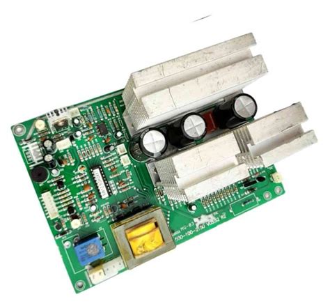
The crimping process is shown in the figure below:
In the HAL/HASL process, due to the uneven thickness of the tin layer and the formation of bow-shaped crystals, the aperture of the crimping hole on the PCB is too small, which is seriously below the lower limit of the aperture tolerance, and ultimately leads to the inability to crimp and assemble normally.
The crimping hole is too small, and the connector Pin cannot be inserted normally. As shown in the figure below, there is another case in the factory where the crimping aperture is too small, resulting in the inability to assemble normally.
Then I will tell you about the assembly process of the welding factory, as shown in the figure below:
We will find that the PCBA process is to mount SMD devices first, then through-hole DIP wave soldering, and finally crimp devices. The previous chips and through-hole devices have been mounted, and finally they cannot be assembled when it comes to crimping. Is it a failure and a waste of time?
Let’s not talk about the final delivery date. The poor A Mao can only gamble on his luck and find 0.3mm PIN pin connector to replace, or… (If you have any good solutions, please tell us at the end of the article)
Summarize in one sentence: For high-speed PCB with crimped components, it is best not to use tin spraying surface, and it is recommended to use immersion gold process.
Finally, the question is:
In the end, A Mao can only find a 0.3mm PIN pin connector to replace, or… What other good solutions do you have? Have you used tin spraying surface treatment when designing PCBs? What other cases have you encountered? Tell us your stories boldly.


