Why is the Clearance from PCB Components to the Edge Important?
Introduction
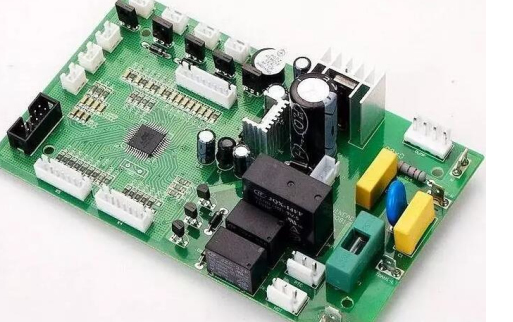
Printed Circuit Board (PCB) design involves numerous critical considerations that affect the functionality, reliability, and manufacturability of the final product. One often overlooked but essential aspect is maintaining proper clearance between components and the edge of the PCB. This clearance—the empty space between any component (including traces, pads, and vias) and the board’s perimeter—plays a vital role in ensuring successful manufacturing, assembly, and long-term operation of the electronic device.
This article explores the multiple reasons why component-to-edge clearance matters, examining implications for manufacturing processes, mechanical reliability, electrical performance, and regulatory compliance. We’ll also discuss industry standards for these clearances and provide practical recommendations for PCB designers.
Manufacturing Considerations
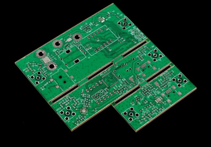
1. Panelization and Depanelization
PCBs are typically manufactured in large panels containing multiple boards that are later separated. Adequate edge clearance is crucial for:
- Routing/Scribing Processes: Most PCB fabrication uses routing or scoring (v-cut) methods to separate boards. These mechanical processes require space near the edges and can cause stress that may damage components placed too close.
- Breakaway Tabs: When breakaway tabs are used for panelization, components near edges may be damaged during the breaking process. A minimum clearance prevents this damage.
2. PCB Fabrication Tolerances
During manufacturing, several processes require edge margin:
- Layer Alignment: Multilayer PCBs can have slight layer-to-layer misalignment during lamination. Edge clearance accommodates these tolerances.
- Copper Etching: The etching process that creates traces has inherent variability, especially near board edges where etchant flow dynamics change.
- Plating Processes: Edge contacts for plating baths require certain clearances for proper electrical connection during manufacturing.
3. Handling During Assembly
PCB assemblers handle boards extensively during:
- Solder Paste Application: Stencil alignment requires edge clearance.
- Pick-and-Place Operations: Robotic handlers often grip board edges.
- Wave Soldering: Conveyor systems contact board edges during transport.
Insufficient clearance risks damaging components during these automated handling processes.
Mechanical and Reliability Factors
1. Mechanical Stress Concentration
Board edges are natural stress concentration points due to:
- Assembly Stress: Insertion/removal from connectors or enclosures flexes edges.
- Thermal Cycling: Different expansion rates between PCB and enclosure create edge stresses.
- Impact/Vibration: External forces typically affect edges first.
Components placed too close to edges experience higher mechanical stress, potentially leading to:
- Solder joint cracks
- Pad lifting
- Component body fractures
- Trace delamination
2. Board Flexure Considerations
All PCBs experience some degree of flexing during:
- Manufacturing handling
- Assembly processes
- End-use conditions
The edges experience the greatest deflection, making nearby components most vulnerable to flexure-induced failures.
3. Mounting and Enclosure Interactions
Proper clearance ensures:
- Enclosure Fit: Components don’t interfere with case walls or mounting features.
- Serviceability: Tools can access edges during installation/removal without damaging components.
- Heat Dissipation: Adequate airflow around board edges prevents thermal buildup.
Electrical Performance Implications
1. Edge Radiation Effects
PCB edges affect signal integrity because:
- Fringing Fields: Electromagnetic fields distort near board edges, affecting high-frequency signals.
- Edge Coupling: Adjacent boards in dense assemblies can couple through edge effects.
- Impedance Discontinuities: Transmission lines near edges experience impedance variations.
2. High Voltage Considerations
For boards with high voltages:
- Creepage/clearance distances from live parts to edges prevent arcing.
- Contamination accumulation near edges increases risk of surface tracking.
3. Grounding and Shielding
Edge clearance affects:
- Edge plating connections
- Shield can placement
- Ground return paths near board periphery
Standards and Industry Guidelines
Various standards specify minimum component-to-edge clearances:
1. IPC Standards
- IPC-7351: Recommends 0.25mm (10mil) minimum for most components
- IPC-2221: Provides general guidelines based on board type and application
- IPC-6012: Qualification requirements addressing edge clearances
2. Manufacturer Capabilities
Most PCB fabricators specify:
- Route/Score Keepout Zones: Typically 0.5-1mm from edge
- Copper-to-Edge Requirements: Often 0.3-0.5mm minimum
3. Application-Specific Requirements
- Automotive: More stringent requirements due to vibration
- Aerospace: Larger margins for high reliability
- Consumer Electronics: Often minimized for space savings
Design Recommendations
Based on these considerations, follow these best practices:
- General Clearance Guidelines:
- Passive components: ≥0.5mm from edge
- ICs and connectors: ≥1mm from edge
- High-voltage parts: Follow creepage/clearance standards
- Critical Areas Requiring Extra Margin:
- Board corners (higher stress concentrations)
- Depanelization edges (v-cut or routing sides)
- Handing edges (where assemblers grip the board)
- Design Verification:
- Use DRC (Design Rule Check) with proper edge clearance rules
- Review manufacturer’s capabilities early in design
- Consider application-specific environmental stresses
- Exceptions and Mitigations:
- When edge components are unavoidable, consider:
- Protective conformal coating
- Reinforced corner/edge constructions
- Alternative depanelization methods (laser cutting)
Conclusion
Maintaining proper clearance between PCB components and board edges is a critical design consideration that impacts manufacturability, reliability, and performance. While the temptation exists to minimize these clearances to save space—particularly in compact consumer devices—doing so without proper analysis risks manufacturing defects, field failures, and compliance issues.
By understanding the multiple rationales behind edge clearance requirements and implementing appropriate design rules, engineers can optimize their PCB layouts for both performance and reliability. As board designs continue pushing size and performance boundaries, thoughtful management of component-to-edge clearances remains an essential aspect of robust PCB design.
The specific clearance values will always involve tradeoffs between board size, cost, and reliability targets, but ignoring edge clearance considerations entirely inevitably leads to problems. Following industry standards while accounting for your specific application requirements provides the best path to successful PCB implementation.