Why PCB Cloning Has Fallen into a Dilemma: A Comprehensive Analysis
Introduction
Printed Circuit Board (PCB) cloning, also known as PCB copying or reverse engineering, has long been a controversial practice in the electronics manufacturing industry. Once considered a quick path to technological catch-up and cost reduction, PCB cloning is now facing unprecedented challenges that have pushed it into a professional and ethical dilemma. This 2000-word article examines the multifaceted reasons behind PCB cloning’s current predicament, analyzing technical, legal, economic, and market factors that have transformed what was once a common industry practice into a problematic approach facing increasing resistance.
The Traditional Appeal of PCB Cloning
To understand why PCB cloning is now in trouble, we must first examine why it was ever popular:
1. Cost and Time Savings: Cloning existing PCB designs eliminated the substantial R&D investment required for original development, providing immediate access to proven circuit layouts.
2. Rapid Market Entry: Companies could quickly bring products to market by replicating successful designs rather than spending months on original development.
3. Technology Acquisition: For developing economies, cloning served as a means to acquire advanced technologies that would otherwise be inaccessible.
4. Maintenance and Repair: Legitimate uses included recreating obsolete boards for equipment maintenance when original designs were unavailable.
However, these short-term advantages have become increasingly overshadowed by the growing problems associated with the practice.

Technical Challenges in Modern PCB Cloning
The evolution of PCB technology has made cloning significantly more difficult and less rewarding:
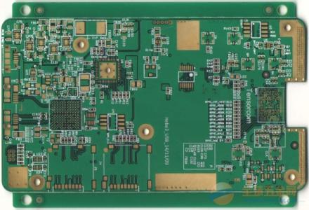
1. High-Density Designs: Modern PCBs with HDI (High Density Interconnect) technology, microvias, and buried/blind vias are extremely difficult to accurately reverse engineer through physical inspection alone.
2. Multi-layer Complexity: Contemporary boards often feature 12+ layers with intricate interconnections that defy easy cloning attempts. The time and equipment required to properly analyze these designs often negates any potential cost savings.
3. Embedded Components: The growing use of embedded passive and active components within the PCB substrate creates invisible elements that cloning might miss, leading to non-functional copies.
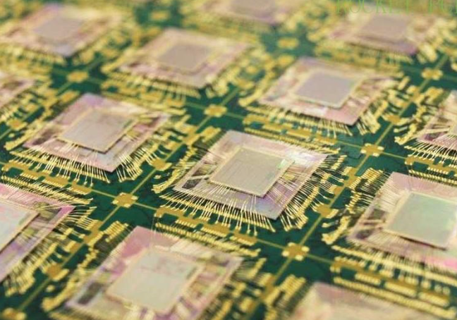
4. Advanced Packaging: Technologies like System-in-Package (SiP) and 3D IC stacking integrate multiple dies in single packages, making circuit analysis from the PCB level alone insufficient.
5. Software Dependencies: Many modern electronics rely heavily on firmware and software that cannot be extracted from physical PCB analysis, rendering cloned hardware useless without the corresponding code.
Legal and Intellectual Property Pressures
The legal landscape has become increasingly hostile to PCB cloning practices:
1. Strengthened IP Protection: Global harmonization of intellectual property laws and more rigorous enforcement, especially in international trade, has raised the risks associated with cloning.
2. Patent Awareness: Many PCB layouts and circuit designs are now explicitly patented, with companies actively monitoring for infringements.
3. Trade Secret Protections: Courts are increasingly recognizing PCB designs as protected trade secrets, leading to successful lawsuits against cloners.
4. Border Enforcement: Customs agencies worldwide are now trained to identify and detain suspected cloned electronics, implementing systems like the U.S. ITC’s exclusion orders.
5. International Treaties: Agreements like TRIPS (Trade-Related Aspects of Intellectual Property Rights) have established global standards that make cloning legally risky across jurisdictions.
Economic and Market Factors
The business case for PCB cloning has deteriorated due to several market developments:
1. Diminishing Cost Advantages: The automation of PCB design and the globalization of manufacturing have reduced the cost differential between original and cloned products.
2. Brand Value Importance: Consumers increasingly prefer authentic brands over clones, willing to pay premiums for guaranteed quality and support.
3. Shortened Product Lifecycles: Rapid iteration in electronics makes cloned products obsolete before they can recoup development costs.
4. Supply Chain Complexity: Modern electronics rely on global supply chains that are difficult to replicate through cloning alone.
5. Quality Expectations: The poor reliability of many cloned products has created market resistance, especially in industrial and professional applications.
Ethical and Reputational Consequences
The professional stigma associated with cloning has grown substantially:
1. Industry Blacklisting: Companies known for cloning face exclusion from professional networks, partnerships, and supply chains.
2. Talent Recruitment Challenges: Engineers increasingly avoid employers engaged in cloning due to concerns about career development and professional ethics.
3. Investor Skepticism: Venture capital and investment communities typically shun companies with cloning-based business models.
4. Certification Barriers: Cloned products often fail to obtain necessary safety and regulatory certifications for target markets.
5. Customer Distrust: Even legitimate companies risk guilt-by-association if their markets become flooded with inferior clones.
Technological Countermeasures Against Cloning
The electronics industry has developed sophisticated anti-cloning protections:
1. Encryption and Authentication Chips: Many designs now incorporate cryptographic elements that prevent operation with cloned PCBs.
2. Obfuscation Techniques: Deliberate layout complexities and misleading markings make reverse engineering more difficult.
3. Unique Identifiers: Serialized components and board-level signatures allow authentication of genuine products.
4. Self-Destruct Mechanisms: Some high-value designs include features that disable operation if tampering is detected.
5. Legal Deterrents: Some firmware includes code that specifically detects and logs cloning attempts for legal evidence.
The Innovation Imperative
Perhaps the most fundamental challenge to PCB cloning is the shifting nature of competition:
1. Performance Demands: Truly competitive products now require optimization beyond what cloning can achieve.
2. Customization Trends: Market demands for tailored solutions don’t align with cloning-based approaches.
3. System Integration: Modern electronics require tight hardware-software co-design that cloned PCBs can’t replicate.
4. Sustainability Requirements: Environmental regulations demand design choices (material selection, energy efficiency) that cloning can’t address.
5. Security Concerns: In an era of cyber threats, cloned electronics pose unacceptable security risks for many applications.
Alternative Approaches to PCB Development
As cloning becomes less viable, more sustainable approaches have emerged:
1. Licensed Production: Legal agreements with original designers for authorized manufacturing.
2. Clean Room Design: Independent development inspired by but not copied from existing products.
3. Open Hardware: Leveraging legitimately shared designs from open-source communities.
4. Contract Development: Partnering with experienced design firms for original solutions.
5. Modular Architectures: Using standardized, legally available modules in custom configurations.
Conclusion: The End of the Cloning Era
PCB cloning finds itself in a professional dilemma because the fundamental conditions that once made it viable have disappeared. What began as legal uncertainties about copying physical board layouts has evolved into comprehensive legal protections. Technical advancements have made successful cloning both more difficult to achieve and easier to detect. Market expectations have shifted toward innovation and quality over mere price competition.
Companies that continue to rely on PCB cloning face mounting legal liabilities, technical failures, and reputational damage. Meanwhile, the electronics industry has developed numerous legitimate alternatives that offer better long-term prospects without the ethical and legal baggage of cloning.
The way forward lies in embracing original design capabilities, licensed technologies, and collaborative development models. For regions and companies that previously depended on cloning, the challenge is to transition to more sophisticated, value-added approaches to electronics manufacturing. While this transition requires investment and cultural change, it represents the only sustainable path in an industry where innovation has become the primary competitive differentiator.
PCB cloning’s current predicament serves as a cautionary tale about the limits of imitation-based development strategies in a world that increasingly values and protects original innovation. The practice that once seemed like a shortcut to market entry has become a professional dead end—a dilemma from which the electronics industry is steadily moving away.