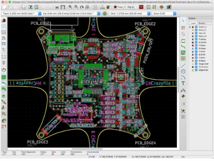
Why Sensitive Traces Near PCB Edges Are Prone to ESD Interference: A Comprehensive Analysis
Introduction
Electrostatic discharge (ESD) represents one of the most persistent challenges in printed circuit board (PCB) design, particularly for sensitive electronic equipment. Among various vulnerable areas on a PCB, traces routed near the board edges demonstrate significantly higher susceptibility to ESD events. This phenomenon has become increasingly critical as modern electronics continue to shrink in size while increasing in complexity and operating frequency. This article examines the fundamental reasons why sensitive traces located near PCB edges are especially prone to ESD interference, exploring the physics behind ESD coupling, the unique characteristics of edge routing, and practical design considerations to mitigate these risks.
Understanding ESD Fundamentals
The Nature of Electrostatic Discharge
Electrostatic discharge occurs when two objects at different electrical potentials come into proximity or contact, resulting in a sudden flow of electricity. Typical ESD events involve voltages ranging from hundreds to tens of thousands of volts, with discharge durations measured in nanoseconds. These transient events can induce both destructive and non-destructive failures in electronic circuits.
ESD Coupling Mechanisms
ESD energy couples into circuits through four primary mechanisms:
- Direct conduction: Physical contact transfers charge directly into components or traces
- Capacitive coupling: Electric field changes induce voltages on nearby conductors
- Inductive coupling: Magnetic field changes induce currents in conductive loops
- Radiated coupling: High-frequency ESD components radiate as electromagnetic waves
For edge-running traces, capacitive and radiated coupling typically dominate the interference mechanisms.

Edge Trace Vulnerability: Key Factors
1. Proximity to External Environment
Traces near PCB edges naturally reside closer to potential ESD sources in the final product enclosure. This reduced physical separation increases exposure in several ways:
- Shorter air gap: Decreases breakdown voltage for air discharge events
- Reduced material barrier: Less dielectric material exists to absorb or block ESD energy
- Increased field strength: Electric fields intensify near sharp edges (edge effect)
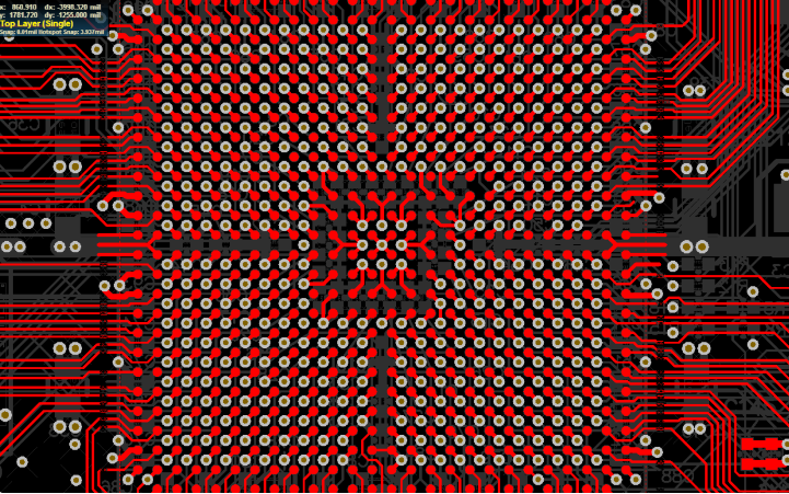
The fringe field concentration at PCB edges can create local field strengths 5-10 times higher than on inner board areas.
2. Lack of Reference Plane Protection
Proper reference planes (typically ground) provide critical shielding against ESD by:
- Creating a low-impedance return path for induced currents
- Shunting high-frequency energy away from sensitive traces
- Forming a Faraday cage effect when properly implemented
Edge traces often suffer from incomplete reference plane coverage because:
- Ground planes typically retract 0.5-1mm from board edges for manufacturing reasons
- Split planes or voids may exist near edges for connector clearance
- The reference plane’s shielding effectiveness diminishes at board peripheries
3. Field Distortion at Board Edges
The dielectric discontinuity at PCB edges causes significant field distortion:
- Field line crowding: Electric field lines concentrate at sharp edges
- Surface wave propagation: Trapped waves can propagate along board edges
- Impedance discontinuities: Changes in trace geometry alter transmission line behavior
These effects create preferential paths for ESD energy to couple into nearby traces.
4. Common Impedance Coupling
Edge traces often share connections with external interfaces, creating shared impedance paths:
- Shared ground returns with I/O connectors
- Common power distribution networks
- Coupled through filter components
An ESD event entering through one port can propagate to sensitive circuits through these shared impedances.

Quantifying the Risk: ESD Coupling at Edges
Capacitive Coupling Analysis
The capacitive coupling between an ESD source and edge trace can be modeled as:
C_coupling ≈ (ε₀ε_r*A)/d
Where:
- ε₀: Permittivity of free space (8.854×10⁻¹² F/m)
- ε_r: Relative permittivity of PCB material
- A: Overlap area between ESD source and trace
- d: Separation distance
For edge traces:
- A increases due to exposed trace sidewalls
- d decreases due to proximity to board edge
Resulting in significantly higher coupling capacitance.
Induced Voltage Calculation
The voltage induced on an edge trace during ESD can be approximated by:
V_induced = (C_coupling * V_ESD)/(C_coupling + C_trace)
Where:
- V_ESD: ESD source voltage (typically 2-15kV)
- C_trace: Trace capacitance to ground
Edge traces typically experience 3-8× higher induced voltages compared to internal traces.
Case Study: USB Data Lines Near Board Edge
Consider USB 2.0 differential pairs (D+ and D-) routed within 2mm of a PCB edge:
| Parameter | Internal Routing | Edge Routing |
|---|---|---|
| Distance to enclosure | 5mm | 1mm |
| Reference plane coverage | Complete | 40% reduced |
| Measured ESD susceptibility | Passes 8kV contact | Fails at 4kV contact |
| Radiated emissions | Compliant | 6dB over limit |
This demonstrates how edge routing dramatically impacts ESD performance.
Design Strategies for Edge-Sensitive Traces
1. Maintain Proper Keepout Zones
Establish clear keepout regions near board edges:
- General signal traces: ≥3mm from edge
- High-speed/sensitive signals: ≥5mm from edge
- Critical analog signals: ≥10mm from edge
2. Implement Edge Shielding Techniques
- Guard rings: Continuous ground traces around board perimeter
- Stitched vias: Ground vias spaced <λ/10 along edges
- Metalized edges: Board-edge plating connected to chassis ground
3. Optimize Layer Stackup
- Extend ground planes to board edges where possible
- Use buried traces instead of surface layers near edges
- Implement power-ground plane pairs at board periphery
4. Proper Filtering and Protection
- Place TVS diodes close to edge connectors
- Implement π-filters for edge-running traces
- Use common-mode chokes for differential pairs
5. Careful Routing Practices
- Avoid right-angle bends near edges
- Minimize parallel run lengths along edges
- Cross board edges perpendicularly when unavoidable
Testing and Verification
Recommended ESD Tests for Edge Traces
- Contact discharge: Direct application to adjacent connectors
- Air discharge: Toward board edge near sensitive traces
- Indirect coupling: Horizontal coupling plane testing
- System-level testing: In final enclosure configuration
Measurement Techniques
- Near-field probes to identify ESD current paths
- Current clamps to quantify coupled energy
- TEM cell testing for radiated susceptibility
- TLP (Transmission Line Pulse) characterization
Future Trends and Challenges
As electronics continue evolving, edge-sensitivity issues are becoming more pronounced:
- Miniaturization: Shrinking form factors force traces closer to edges
- Higher frequencies: 5G and mmWave signals are more ESD-sensitive
- Flexible electronics: Dynamic bending alters edge coupling effects
- Advanced materials: Low-k dielectrics may increase edge coupling
Emerging mitigation approaches include:
- Active edge cancellation circuits
- Nanocomposite edge coatings
- 3D-printed edge shielding structures
- Machine learning-assisted edge routing algorithms
Conclusion
Sensitive traces routed near PCB edges face substantially increased ESD risks due to fundamental physical principles including field concentration, reduced shielding effectiveness, and enhanced coupling mechanisms. The combination of environmental exposure, geometric effects, and material discontinuities creates a perfect storm of vulnerability at board peripheries. Through careful design practices including proper keepout zones, optimized layer stackups, and targeted protection strategies, designers can effectively mitigate these risks while meeting ever-more-challenging space constraints. Understanding these edge effects enables more robust PCB designs capable of withstanding real-world ESD threats while maintaining signal integrity in sensitive circuits.