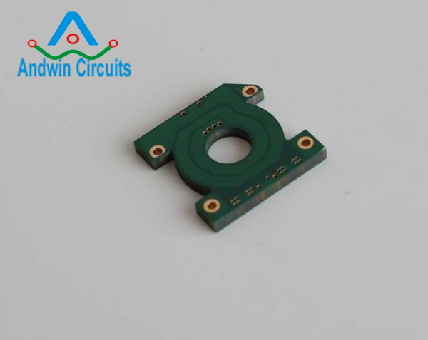
Heavy Copper PCB
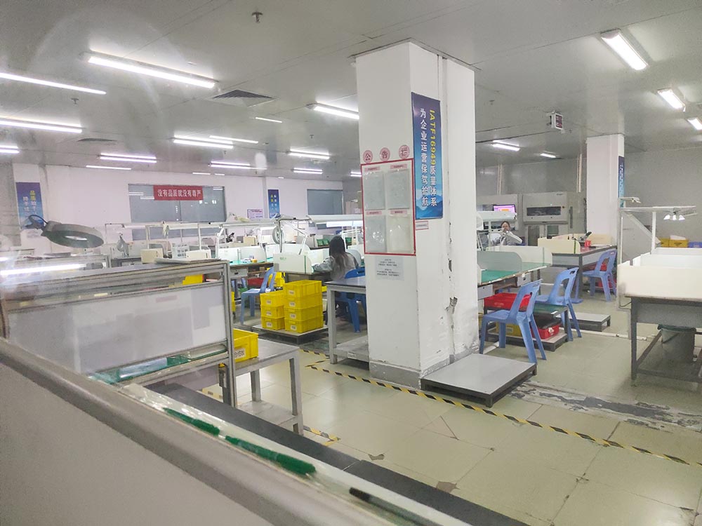
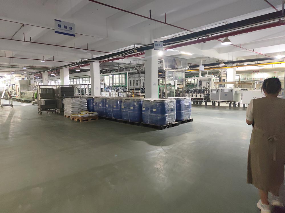
As a leading in heavy copper PCB manufacturers,
Andwin PCB have rich experience in heavy copper pcb fabrication
We are 20 years heavy copper PCB factory and competitive price
Heavy copper PCB product
We have capability to make selective thicker copper in same layer,
Andwin could meet all of your Heavy copper PCB special requirement.
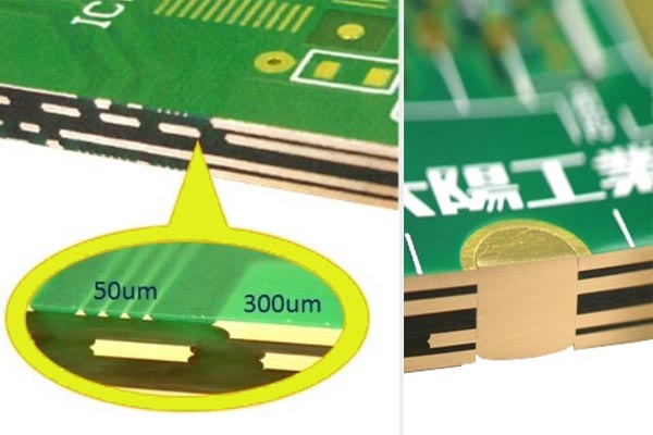
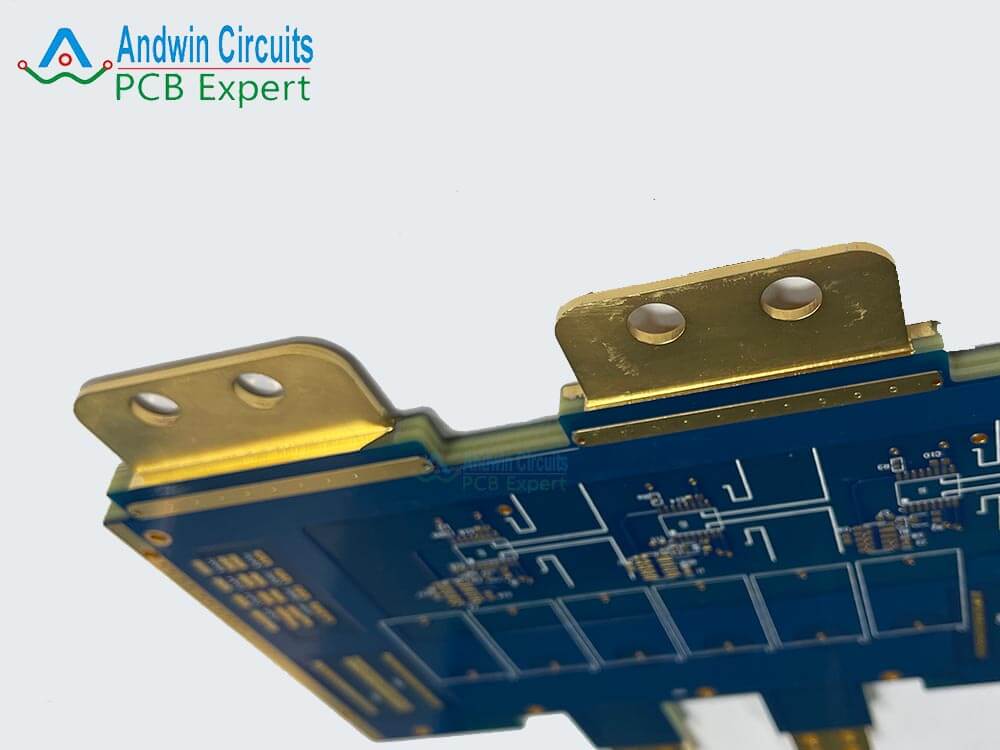
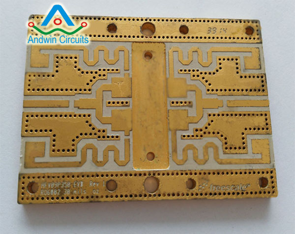
4 layers heavy copper circuit board
1.0mm copper thickness
heavy copper printed circuit board
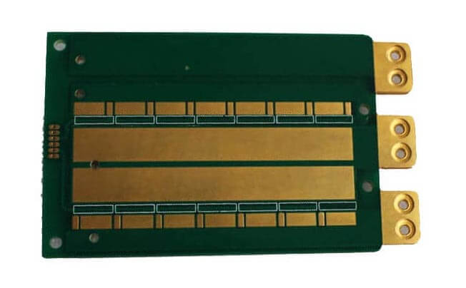
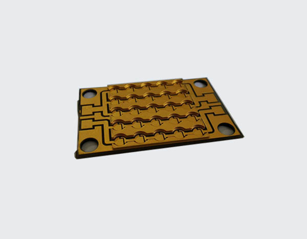
Selective heavy copper PCB
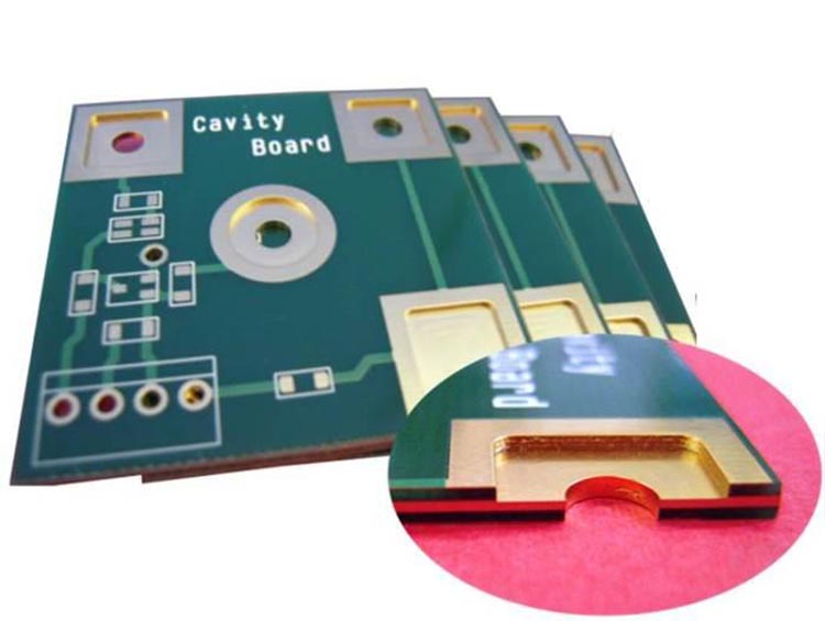
Heavy copper PCBs with sink depth slot
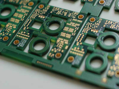
Heavy copper PCB
Heavy copper AIN Ceramic PCB
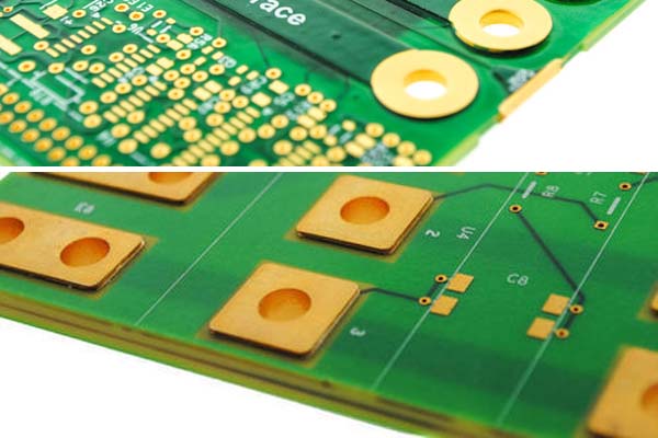
Heavy Copper and copper Coin PCB
Heavy Copper PCB capabilities
Based on the requirement, heavy copper PCBs can be expensive to produce.
Thus, it is more complex in design but more effective in producing heavy copper PCB.
It should have the following capabilities:
The copper thickness up to 40 OZ ( 1400um )
The base material consists of FR4 / Aluminum / Copper / Ceramic
The outline should be made of routing, punching, and V-Cut
The solder mask comes in white, black, blue, green, or red in oil
The surface finishing Immersion Gold, HASL and OSP
Maximum panel size must be 580*480mm
More Knowledge about Heavy copper printed circuit boards
Heavy copper PCB refers to a type of printed circuit board (PCB) that is designed with thicker copper traces and planes compared to standard PCBs.
The copper thickness in heavy copper PCBs typically ranges from 3 ounces per square foot (oz/ft²) to 20 oz/ft², or even higher in some cases,
Andwin have experience make the heavy copper PCB up to 40 ounces.
The boards are manufactured by acquiring various etching and plating techniques and the goal is to add copper thickness to the plated holes and sidewalls.
The purity of copper is determined according to the weight, thickness of plating and proper substrate.
It also determines the strength of the PCB in the through-holes that can turn a weak board into a long-lasting one to perform in a dependable wiring platform.
Therefore, the thickness of the copper always needs to be measured during the circuit designing state in order to consider how much it can serve through operations.
The compatibility is assured by the resolution of current-carrying capacity measured by the width and thickness of heavy copper.
The increased copper thickness in heavy copper PCBs allows for higher current-carrying capacity and better heat dissipation.
This makes them suitable for applications that require high power or high reliability,
Such as power electronics, automotive electronics, aerospace systems, and industrial equipment.
Heavy copper PCBs are also used in applications where thermal management is crucial,as the increased copper mass helps in dissipating heat generated by power components.
Additionally, the thick copper layers provide better mechanical strength and durability to the PCB, making it more resistant to thermal stress and mechanical shocks.
The increased copper thickness in heavy copper PCBs allows for higher current-carrying capacity and better heat dissipation.
This makes them suitable for applications that require high power or high reliability,
Such as power electronics, automotive electronics, aerospace systems, and industrial equipment.
Heavy copper PCBs are also used in applications where thermal management is crucial,
As the increased copper mass helps in dissipating heat generated by power components.
Additionally, the thick copper layers provide better mechanical strength and durability to the PCB,
Making it more resistant to thermal stress and mechanical shocks.
Overall, heavy copper PCBs offer enhanced performance and reliability for demanding applications that require high power handling, efficient heat dissipation, and robust construction.
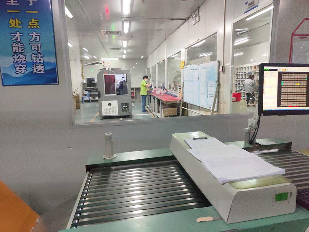
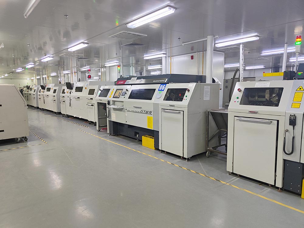
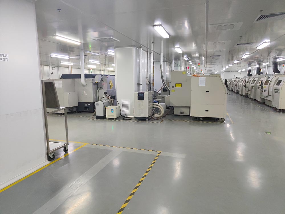
The manufacturing processes of heavy copper PCB intake the combination of multiple processes enabling extreme copper thickness requirements.
No matter single or double-sided PCBs, both need to go through the process of etching and plating.
The etching sheets of copper foil are the beginning of putting circuit layers.
Then the unwanted etched copper is removed and the plates are settled for adding thick layers of coppers to planes, traces, pads and plated-through holes.
After that, the entire circuit is being laminated into a complete package by using an epoxy-based substrate.
The PCBs are incorporated with heavy copper circuits to produce specialized etching and plating techniques.
Generally, the properties are formed completely by etching thick copper-clad laminated with the board material.
This creates uneven trace sidewalls and unacceptable undercutting.
The plating technology is getting advanced that allows heavy copper features to form with a combination of plating and etching.
This results in straight sidewalls and negligible undercuts.
While designing a heavy copper PCB, the factors of thermal stress are the prime interest and,
Engineers endeavor to hit the roof for the thermal pressure as much as possible.
The procedure of production goes into a progression period with various PCB technologies including Aluminum PCB.
This has been invented due to the capability of handling thermal stress.
The power budget can be minimized by preserving circuit performance and makes it environment-friendly design consisting of thermal sinking quality.
This is the actual concern while a heavy copper PCB is being designed
Any electronic gadgets with an overheating issue result in failure or go through life-threatening hazards.
Therefore, the thermal management system is paramount.
Generally, the heat sinking quality is measured according to the achievement of external heat sink usage of the heat-producing components.
The approach of such component connects according to the high temperature.
If the heat distribution is not desolated, then due to the dissolution of heat,
It will consume the sinking heat from the component and transfer to the surroundings.
Normally, the heat sinks are made of copper or aluminum but the development costs for the usage of heat sinks along with the demand for space and time are exceeding.
On the other hand, in heavy copper PCB, the heat sinks are being printed on the board at the time of assembling because it serves better than the usual heat sink.
Also, the limitations are less for the placement of heat sink while the external heat sinks entail extra space.
• High thermal tolerance capacity
• Outstanding current carrying capacity
• Eliminates the complex wired bus configuration
• Condensed circuit size in order to combine several copper weights at the same PCB
• Usage can be optimized due to high-temperature materials for a lower probability of circuit failure
• Due to the improvement of mechanical characteristics, tropical materials are used in PCB
• Heavy copper deposition in some specific areas can be linked to the cold plate interfaces to serve heat sinks
• Product size remains compact for several copper weights for the same circuit layers
• Incorporated multiple copper weights have the same layer of circuitry
• Transforms onboard high-power-density
• Heavy copper-plated vias pass through the elevated current for the PCB
• Assists heat transfer for the outer sink
• Integrates high-current circuits to control circuits on a single PCB
• Selective areas are plated with heavy copper functioning the built-in heat sinks or cold sinks
• Power supplies and power converters|
• Torque controls
• Solar power convertersSafety and signal systems
• Power distributionPower line monitors
• Wielding equipment
• Rail traction systems
• UPS systems
• Protection relays
• Storage pumping plants
• Overload relays
• HVAC systems
• High power rectifiers
• Excitation systems for power regulators
• Position control systems
• Nuclear power applications
• Line reactors
• Hydro-electric plants
• Surge protectors
• Fuse blocks
• Weapons control systems
The famous brand Heavy copper PCB customers

Western Digital Honeywell
Get professional PCB solution from us!
Please send us email: sales@andwinpcb.com ( priority ) with your PCB file and specification detail,
Our teams will quote to you as soon as possible,
Or fill follow form our team will contact you soon.