3D pcb printing
With supply disruptions and design constraints often faced in circuit board production, more and more suppliers are turning to 3D printers to solve these problems. Compared with traditional production methods, 3D printed circuit boards (PCBs) are faster to manufacture, more versatile, and can produce more complex circuits while achieving significant cost savings. The biggest appeal of 3D PCBs today is that they give manufacturers control over their circuit board supply and eliminate factory downtime, shipping slowdowns, etc.
What are 3D printed circuit boards?
3D PCB technology is new to the electronics industry but has developed rapidly in recent years. Specialized circuit board 3D printers can make circuit boards much faster than traditional methods, and for some applications, they can even be made using ordinary desktop FDM 3D printers with conductive filament. Traditional circuits may take days or months to produce, while 3D printers can produce functional circuit boards in 30 hours or less.
Design freedom is another benefit, and 3D printers can create circuits that are much more complex than traditional rectangular boards, including flexible boards, honeycomb structures, and even fully three-dimensional boards.
PCB 3D printing technology generally works in two ways: printing circuits directly with conductive material or printing circuit boards with hollow channels or trenches that are later filled with conductive material. Let’s take a closer look at how these methods differ.
Circuit board 3D printers build entire circuit boards through additive manufacturing. This is different from traditional PCB production methods, which usually use mechanical means to etch circuits into the board or CNC mill conductive traces.
●Method 1: Conductive materials
PCB 3D printers using conductive materials lay down conductive materials to form circuits. Conductive materials are inks or filaments infused with conductive particles such as silver, copper or graphite, which can also be sprayed as a stream of material loaded with aerosols.
Ink is the more common choice in commercial PCB 3D printers. Inkjets similar to those in 2D printers can be used to deposit droplets of conductive and insulating inks to build up circuits. Some printers require pre-made substrates, while others can print the entire substrate from scratch. The latter can produce complex multi-layer double-sided circuit boards that can realize embedded components such as coils, resistors or LEDs.
Conductive filaments are another option for printed circuit boards. Users can print these filaments with almost any FDM printer, which is more cost-effective. However, the circuit will be bulkier and less efficient than an ink-based PCB. Therefore, conductive filaments may not be suitable for commercial operations, but they are ideal for prototypes.
●Method 2: Hollow channels
The second method produces a circuit board with hollow channels where the circuit is located. Essentially, you will print a “housing” to contain the conductive material that you deposit into the channels after printing. In order for the circuit to work properly, you must print the circuit board with a non-conductive filament such as ABS or PLA.
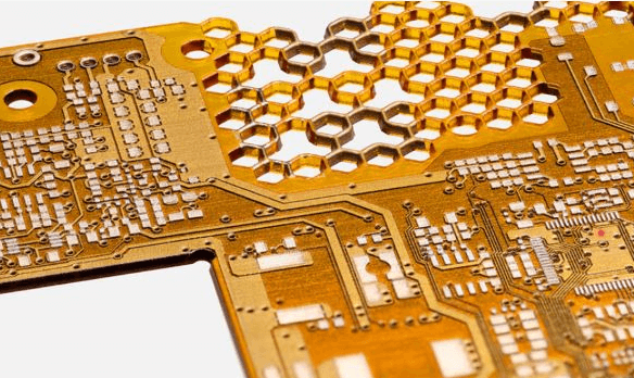
△ This circuit carrier is 3D printed by EOS on a selective laser sintering machine, and then the circuit channels are filled with conductive material (Source: EOS)
This method enables you to create a PCB using almost any 3D printer that is accurate enough. Therefore, it is a very economical solution. It can also provide higher conductivity than some directly printed circuits, especially those made with conductive filaments. For example, PCB manufacturer Beta LAYOUT relies on a selective laser sintering machine from EOS to 3D print circuit carrier conductor tracks, which are then filled with conductive material.
Advantages and Disadvantages of PCBs
△ Custom tools and fixtures used for traditional circuit board manufacturing are manufactured using 3D printing of static-safe materials, such as Impossible Objects’ nylon board fixture (Source: Impossible Objects)
3D printing PCBs can offer significant advantages over traditionally manufactured circuit boards, but it also has some very real limitations. As a result, it may not yet be an ideal technology for all purposes.
● Advantages
- Cost-effectiveness: While some PCB 3D printers are costly, they can quickly pay back on investment. 3D-printed PCBs consume less material. In addition, 3D printing eliminates shipping and outsourcing costs, which can make circuit prototyping significantly cheaper.
- Production speed: With 3D printers, PCB production time is measured in hours. They can speed up the entire process, including circuit design, prototyping and iteration, end-use production and market promotion.
- Design freedom: PCBs produced with 3D printers can be of any shape and can also be printed with flexible materials. This allows for greater design freedom, allowing engineers to focus on developing lighter, smaller, and more efficient products.
- Reduced waste: Traditional production methods generate a lot of waste. 3D printed PCBs can make circuits more compact, complex in shape, and save materials.
- On-demand production: 3D printing is able to produce circuit boards as needed without having to keep large inventories. At the same time, you don’t have to take on large orders from third-party manufacturers, and it also eliminates the chance of supply chain disruptions.
- High precision: 3D printers can achieve higher precision in PCB production than traditional methods. Some printers can even place components, further reducing the possibility of human error in the production process.
- More layers: When you use an additive manufacturing system for multi-layer PCBs, your board geometry can be more complex.
● Disadvantages
- Limited materials: As a relatively new technology, 3D PCB printing does not yet have a wide range of materials. Many printers can only use one or two materials provided by the manufacturer, which can increase costs and limit design options.
- Lower conductivity: Despite the continuous advancement of PCB 3D printing, some conductive printing materials do not perform as well as traditional materials.
- Limited board size: 3D printers can only produce PCBs as large as their print chamber can accommodate (this is not a problem for most applications). Since the print chambers of many PCB 3D printers are quite small, they are not suitable for producing large boards.
- Lack of choice: Just like materials, there are currently few companies that produce PCB 3D printers commercially. This situation will most likely improve as the technology matures, but for now, there is not a wide range of choices.
Applications of 3D Printed Circuit Boards
3D PCBs already have a wide range of applications, and many manufacturers have successfully produced PCBs for various industries ranging from education to advanced aerospace equipment.
● 3D PCBs for biomedical research
The research team at Stanford University in California is developing new alternative electronics, such as flexible and biocompatible electronics. Postdoctoral researcher Dr. Naoji Matsuhisa is developing stretchable sensors for the next generation of biomedical wearable devices.
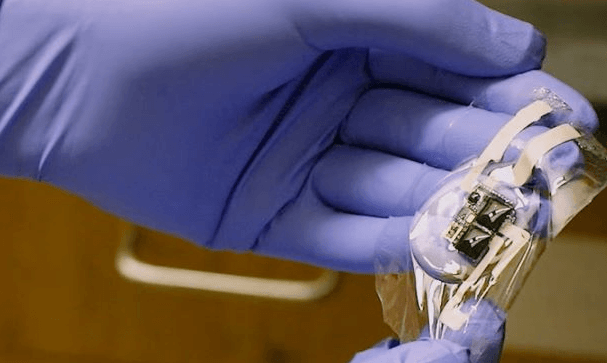
△Stanford University uses flexible 3D PCBs to study biocompatible inks for robotic skin and biomedical wearable technology (Source: Voltera)
Many devices have sensors placed on elastic, extremely flexible substrates to keep them as close to the skin as possible. These sensors must then be connected to rigid circuit boards. The connection points must also be able to stretch for comfortable wear and the highest degree of functionality. Bao Research uses Voltera’s V-One 3D printer to produce stretchable conductors for connecting components. The V-One enables Bao Research Group to quickly manufacture the unusual circuits and connectors they need.
●3D printed solar cells for renewable energy
The Fraunhofer Institute for Solar Energy Systems ISE is a research center based in Germany that conducts scientific and engineering research and development to advance solar and photovoltaic power production technology. They use Optomec’s aerosol jet (AJ) 3D printing system to produce solar cells on Fz wafers. 3D printing technology enables Fraunhofer ISE to print fine feature collector lines with widths between 18 and 60 microns using silver-infused inks. This layer is then covered in a surface layer consisting of multiple conductive materials.
△ Visualization of a photovoltaic roof with shingled solar cells (Source: Fraunhofer ISE)
Compared to previously used cells, 3D printed solar cells have higher conductivity and lower shading effects. The technology helped Fraunhofer ISE increase the efficiency of its solar cells by 20%. With the success of the technology, several commercial solar cell manufacturers have adopted it to develop more efficient solar cells for green energy production.
●Aerospace and Military
Phased array antennas are complex arrays of antenna elements that allow operators to change the direction of their radiation without moving the antenna. This can be achieved by controlling the phase of each antenna element signal so that it can “aim” at a specific point. These devices are critical in aerospace and military applications to facilitate secure communications.
Florida-based engineering company Sciperio has successfully developed a method for printing complex multi-layer RF electrical structures on curved surfaces in collaboration with the U.S. Air Force Research Laboratory (AFRL). This enables the company to produce phased antenna arrays for aircraft and other aerospace and military applications. Key to the success of the project was the nScrypt 3Dn series Factory in Tool (FiT) 3D manufacturing system. The 3Dn FiT system combines FDM 3D printing with micro dispensing, aerosol jetting and component placement, enabling Sciperio to manufacture the complex structured electronics required for the curved antenna array.
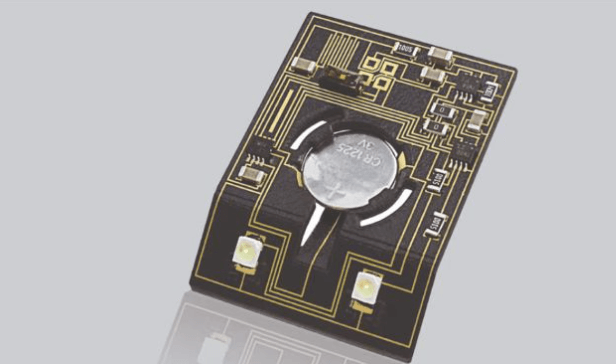
● Rapid prototyping
Phytec, based in Mainz, Germany, is a leader in industrial embedded electronics. Due to the custom nature of many of its products, Phytec needs to be able to quickly prototype, test and produce new technologies.
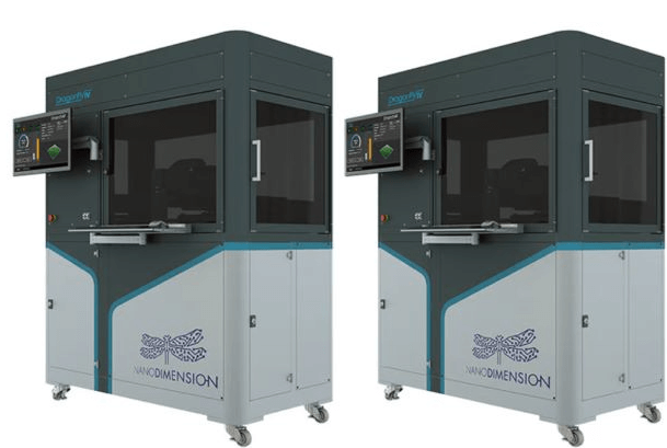
△ Functional PCB touch sensor 3D printed on Nano Dimension’s DragonFly Pro (Source: Sven Dengel, Phytec)
Traditional production methods often result in extremely long lead times for prototypes – up to 50 days. Phytec wanted to shorten development cycles and improve product quality. To do this, it was one of the first commercial companies to adopt Nano Dimension’s DragonFly 3D printer. This decision quickly proved to be the right one. Thanks to DragonFly, Phytec is now able to produce high-quality PCB prototypes in-house within a single working day. Its engineers can identify potential errors and issues early in the PCB design process, saving development time and materials. In addition, the 3D printing process enables Phytec to explore new ideas, unlocking creative PCB structures that were previously unattainable.
“Depending on the size and complexity of the board, it takes us 12 to 18 hours to print a PCB. This is 10 to 15 times faster than ordering PCBs in the traditional way. As a result, within a single working day, the first new PCB of a new design is available in our production facilities”, says Bodo Huber, Phytec’s CTO.
3D PCBs: State-of-the-art
△ This fully 3D manufactured printed cylindrical circuit created by nScrypt features an embedded Bluetooth microcontroller, a printed antenna, and a range of fully embedded sensors and components, such as acoustic, light, and motion sensing (Source: nScrypt)
R&D in 3D PCBs is ongoing in a variety of sectors across a variety of industries. Here are some of the most promising developments.
A major development demonstrated at the 2022 IPC APEX Expo, the premier PCB conference, is moving beyond circuit boards to printed circuit structures (PCS). Engineers are realizing that they can go beyond flat sheets and make circuits in nearly any shape. For example, 3D printed circuit cylinders were one of the demonstrations at ICP APEX. These new shapes could help manufacturers fit PCBs into smaller spaces and produce them more cheaply. While the technology isn’t ready for commercialization yet, it points the way to where the industry is headed.
Meanwhile, researchers at the University of Houston announced in June 2022 that they had created a new 3D printing resin infused with organic semiconductor materials. Using this resin, the research team successfully printed objects such as micro-printed circuit boards. The discovery could pave the way for small bioactive electronics that could be used in wearable sensors, prosthetics, implanted neural chips, and other medical devices.
Additive PCB manufacturing for alternative etching processes. In August 2022, a collaboration between German companies InnovationLab and ISRA VISION reported a breakthrough in 3D PCBs. The two created a working physical prototype using a novel 3D printable copper ink. The multi-layer PCB is compatible with traditional reflow soldering, allowing manufacturers to install c omponents without purchasing any new equipment.
△InnovationLab has made a breakthrough in additive manufacturing of printed circuit boards, meeting higher environmental standards for electronic production while also reducing costs (Source: InnovationLab)
Dr. Janus Schinke, head of printed electronics at InnovationLab, said: “This is a state-of-the-art production process that will reduce costs and reduce logistics dependence on suppliers, while providing three key benefits to the environment: consuming less material, using less energy and generating less waste. By the end of 2022, we hope to scale up this process to large quantities to meet customer requirements for more than 1 million strips.” The substrate used by InnovationLab 3D PCB is 15 times thinner than traditional technology, resulting in reduced material consumption and significantly less waste in the production process.
Top circuit board printers
Compared to more mature 3D printing technologies, the 3D printed PCB market is currently very small. Here are some highlights of the currently available PCB 3D printers.
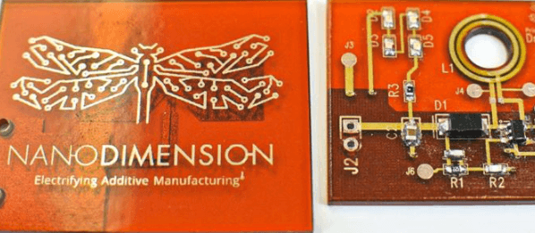
●Nano Dimension
△Nano Dimension DragonFly IV (Source: Nano Dimension)
Nano Dimension’s DragonFly, launched in 2015, was hailed as the world’s first desktop-size 3D printer for producing professional-grade PCBs. The company’s current product – the DragonFly IV – doesn’t fit on a desk, but it’s still a powerful solution for AME production. The DragonFly IV deposits two specialized inks onto the print bed. The first of these is AgCite, an ink filled with conductive pure silver nanoparticles. AgCite provides predictable conductivity for PCBs even at a 75-micron layer height. The second ink consists of a dielectric polymer that can create PCB structures with an 18-micron layer thickness.
The DragonFly IV can deposit these inks simultaneously and cure them using infrared and ultraviolet light. This printer can create high-performance devices and circuits, even with complex 3D shapes. Nano Dimension’s Flight software integrates seamlessly with DragonFly IV, making it easy to launch print jobs. Flight enables users to control everything from data preparation and printability verification to the actual printing process. DragonFly IV is also powered by DeepCube, Nano Dimension’s proprietary AI solution for additive manufacturing. DeepCube uses the same principles as voice or image recognition AI to identify tiny defects that are invisible to the human eye and detect them in real time.
Correcting printing errors improves part quality and output. DeepCube connects to 3D printers around the world and learns to improve efficiency and accuracy with each print run. In addition to DragonFly IV, Nano Dimension also offers the Fabrica 2.0 micro 3D printer, which can serve electronics manufacturers by creating micro connectors and other micro components.
●Voltera
△Voltera circuit board 3D printer (Source: Voltera)
Voltera One is a compact PCB 3D printer that focuses on ease of use and fast production. It is an affordable machine that will not break the budget of even small and medium-sized businesses. V-One provides an all-in-one PCB production package. It is capable of dispensing conductive ink, drilling holes in the circuit board, heating and curing ink, and reflow. Voltera’s magnetic heads are easily replaced, and the magnetically mounted magnetic heads simply pull down and snap into place in seconds without any tools.
Instead of printing the entire circuit board, V-One relies on pre-made circuit boards. Users must purchase the circuit boards separately, but you are free to choose their materials because V-One is substrate-agnostic. Voltera offers standard and flexible conductive inks, enabling users to print PCBs for a variety of applications. After placing the circuit board in the printer, the V-One aligns the print head height and begins depositing the conductive ink, which is then finally cured. The machine works quickly and can produce a simple single-layer PCB in 2-3 hours. The V-One can currently produce two-layer boards, but Voltera hopes to add more multi-layer support in the future.
●BotFactory SV2
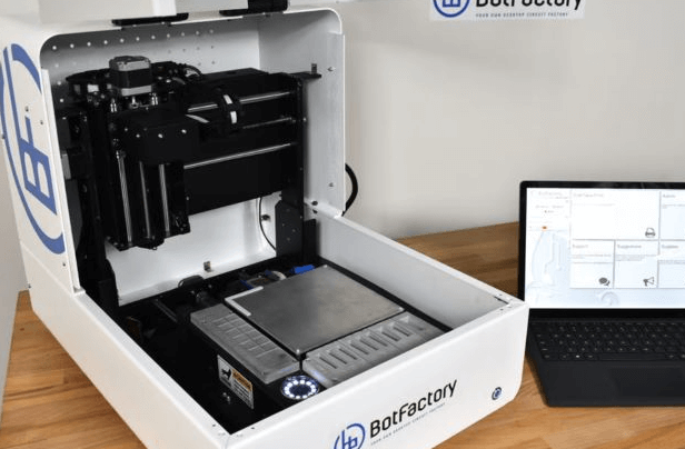
△BotFactory’s SV2 is an all-in-one desktop printer (Source: BotFactory)
BotFactory’s first PCB printer had a cute name, Squink, which came out in 2015 and competed with Nano Dimension’s DragonFly for the title of the first desktop PCB printer. . Squink is now discontinued and BotFactory has replaced it with the more professional SV2.
The SV2 is an all-in-one desktop printer specifically targeted at research and engineering applications. The machine can print multi-layer circuits with conductive and insulating inks and deposit solder paste. In addition to conductive and resistive inks, BotFactory has created a resistive ink for the SV2. This material allows manufacturers to print resistors directly onto PCBs without installing a separate resistor component.
The printer is available in Starter, Enhanced, and Professional versions. The Starter and Enhanced models can print up to two layers, while the Professional model is capable of creating four-layer PCBs. The minimum gap range for the printer models is 400 to 300 and 200 microns, respectively.
●nScrypt 3Dn
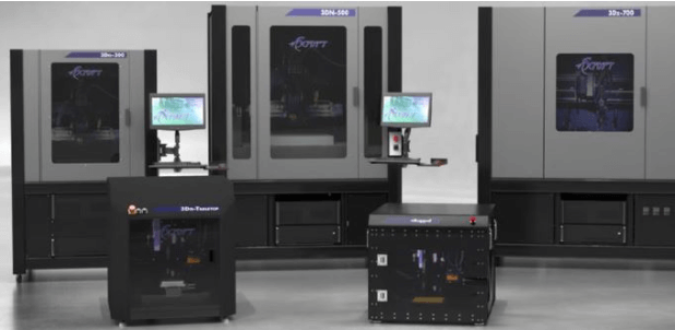
△FiT system, source: nScrypt
FiT machines are equipped with FFF 3D printers, and they are also capable of micro-dispensing, drilling, polishing, and placing components using 1-5 replaceable tool heads (or gadgets, as manufacturers call them). nScrypt says that the 3Dn series of FiT machines, with automatic tool changes, post-processing methods, and claimed support for more than 10,000 materials, are suitable for making products, not just parts.
PCB producers are particularly interested in FFF printing and micro dispensing capabilities. Using a FiT machine, it is possible to 3D print the structure and housing of a device while also producing embedded conductive traces as thin as 20 microns. This allows the production of what nScrypt calls printed circuit structures, 3D printed objects with embedded circuits. The 3Dn series of FiT printers are available in desktop sizes and gantry platform models.
●Optomec Aerosol Jet Flex
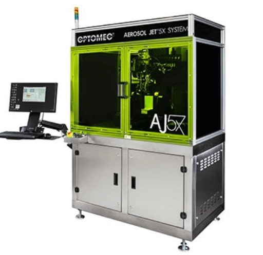
△Optomec’s Aerosol Jet Flex 3D printer (Source: Optomec)
New Mexico-based Optomec has created a unique solution for additive manufacturing of PCBs and other electronics. The technology, called aerosol jetting (AJ), can print conductive traces on 2D and 3D substrates. AJ can create interconnects in 2D applications, simulating multi-layer circuit boards on a single layer by using dielectric materials at the intersection of the circuits. The technology can also print circuits directly on 3D surfaces without wire bonding.
Optomec’s flagship machine is the Aerosol Jet Flex 3D printer. It can be configured with three to five axes of motion and can print features as small as 10 microns and layer heights as low as 100 nanometers. The printer also has a print chamber that is appropriately sized for a PCB 3D printer, with a maximum build volume of 350 x 250 x 300 mm. Electronics manufacturer Lite-On Mobile uses the technology to 3D print antennas onto mobile phones.
The AJ Flex uses an atomizer to turn its ink-based materials into a dense aerosol mist. The mist is delivered to the print platform via a deposition head, where a sheath gas focuses the aerosol into a highly concentrated beam. This method can print circuits on plastic, ceramic, or metal substrates. Optomec offers a variety of add-on modules for the AJ Flex. The laser sintering module can sinter metallic inks at room temperature, while the UV curing module allows operators to cure UV-sensitive polymers to create 3D structures. As the name implies, the full-featured printhead unlocks extended print feature sizes up to 2800 microns.
Circuit board 3D printing services
△ Circuit board printed by Beta Layout (Source: Beta Layout)
PCB 3D printers require a large upfront investment and may not be for everyone. Fortunately, it is possible to 3D print PCBs without purchasing your own machine. PCB 3D printing services allow you to order PCBs for prototyping and end-use.
●Nano Dimension
In addition to manufacturing the DragonFly 3D printer, Nano Dimension also provides PCB design and manufacturing services. The company has printing labs around the world, enabling it to provide turnaround times measured in days. Nano Dimension engineers can also work with customers to design and customize PCBs and high-performance electronic devices from scratch to suit a variety of applications.
●Beta Layout
Beta Layout specializes in 3D printing and manufacturing PCB prototypes. The company combines its two areas of expertise to provide 3D mechatronic device (3D-MID) prototyping services. Beta Layout can 3D print complex objects with integrated circuits. Its technology enables the miniaturization of electronic components and allows manufacturers to prototype innovative circuit structures faster than traditional production methods.
●Phytec New Dimensions
Phytec New Dimensions, a subsidiary of Phytec, offers PDB 3D printing using Nano Dimension’s DragonFly technology. The company focuses on producing proof-of-concept PCBs and provides assembled PCBs and individual design studies to determine the 3D printing feasibility of a project. Phytec promises fast turnaround times, with the ability to print a complete prototype within two working days.