4-layer PCB Design: From Basics to Advanced Applications
Introduction
Printed circuit boards (PCBs) are the core components of modern electronic devices, responsible for connecting and supporting various electronic components. As the complexity of electronic devices continues to increase, single-layer and double-layer PCBs can no longer meet design requirements. 4-layer PCBs have become the first choice for many complex electronic devices due to their higher wiring density, better signal integrity, and electromagnetic compatibility (EMC). This article will delve into the design, advantages, application scenarios, and key issues that need to be paid attention to during the design process of 4-layer PCBs.
1. Basic Structure of 4-layer PCBs
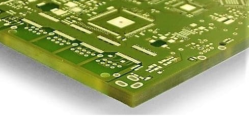
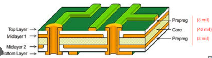
A 4-layer PCB consists of four layers of conductive material (usually copper) separated by insulating materials (usually FR-4). A typical 4-layer PCB structure includes the following layers:
- Top Layer: This is the top layer of the PCB, usually used for placing components and signal routing.
- Inner Layer 1: This is the first inner layer, usually used as a power layer or ground layer.
- Inner Layer 2: This is the second inner layer, usually used as a signal layer or power layer.
- Bottom Layer: This is the bottom layer of the PCB, usually used for placing components and signal routing.
2. Advantages of 4-layer PCBs
2.1 Higher routing density
4-layer PCBs provide more routing space, allowing designers to implement more complex circuit designs on a smaller board area. This is especially important for high-density interconnect (HDI) applications.
2.2 Better signal integrity
By placing the power and ground planes on the inner layers, 4-layer PCBs can effectively reduce signal noise and crosstalk, thereby improving signal integrity. This is especially important for high-speed digital circuits and radio frequency (RF) circuits.
2.3 Improved electromagnetic compatibility (EMC)
The power and ground planes of 4-layer PCBs can effectively shield the signal layer and reduce electromagnetic interference (EMI), thereby improving the electromagnetic compatibility of the device.
2.4 Better thermal management
The power and ground planes of a 4-layer PCB can effectively disperse heat, thereby improving the heat dissipation performance of the circuit board. This is especially important for high-power applications.
3. Design process of a 4-layer PCB
3.1 Demand analysis
Before designing a 4-layer PCB, you first need to clarify the design requirements, including circuit functions, performance indicators, size restrictions, cost budgets, etc.
3.2 Schematic design
Based on the results of the demand analysis, design the circuit schematic. The schematic is the basis of PCB design, and it is necessary to ensure the correctness of all components and connection relationships.
3.3 PCB layout
In the PCB design software, layout components according to the schematic. Reasonable layout can effectively reduce the signal path length and improve signal integrity.
3.4 Routing
After the layout is completed, perform signal routing. The routing of a 4-layer PCB usually includes the top layer, bottom layer, and two inner layers. Reasonable routing strategies can effectively reduce signal noise and crosstalk.
3.5 Power and Ground Plane Design
In a 4-layer PCB, the power and ground planes are usually placed on the inner layer. Reasonable design of the power and ground planes can effectively improve signal integrity and electromagnetic compatibility.
3.6 Design Rule Check (DRC)
After the routing is completed, the design rule check is performed to ensure that the PCB design meets the manufacturing and performance requirements.
3.7 Generate Manufacturing Files
Finally, generate PCB manufacturing files, including Gerber files, drilling files, and assembly drawings.
4. Key Issues in 4-layer PCB Design
4.1 Signal Integrity
In high-speed digital circuits, signal integrity is a key issue. Signal integrity can be effectively improved by reasonably designing the power and ground planes, using differential pairs and impedance matching, and other technologies.
4.2 Electromagnetic Compatibility (EMC)
Electromagnetic compatibility is another key issue. Electromagnetic interference can be effectively reduced by reasonably designing the power and ground planes, and using shielding and filtering techniques.
4.3 Thermal Management
In high-power applications, thermal management is a key issue. Heat dissipation can be effectively improved by properly designing power and ground planes, using heat sinks and thermal vias, and other technologies.
4.4 Manufacturing Process
The manufacturing process of 4-layer PCBs is more complex than that of single-layer and double-layer PCBs, requiring higher precision and stricter quality control. Therefore, the limitations of the manufacturing process need to be considered during the design process.
5. Application Scenarios of 4-layer PCBs
5.1 Communication Equipment
4-layer PCBs are widely used in communication equipment such as routers, switches, and base stations. These devices usually require high-speed signal transmission and high-density wiring.
5.2 Computer Hardware
4-layer PCBs are also widely used in computer hardware such as motherboards, graphics cards, and storage devices. These devices usually require high-density wiring and good signal integrity.
5.3 Consumer Electronics
4-layer PCBs are also widely used in consumer electronics, such as smartphones, tablets, and smart home devices. These devices usually require miniaturization and high-density wiring.
5.4 Industrial Control
4-layer PCB is also widely used in industrial control equipment, such as PLC, industrial robots and automation equipment. These devices usually require high reliability and good electromagnetic compatibility.
6. Future Development Trends of 4-layer PCB
6.1 High-density interconnect (HDI)
With the miniaturization and complexity of electronic devices, high-density interconnect (HDI) technology will become an important trend in 4-layer PCB design. HDI technology can further improve wiring density and reduce board area.
6.2 High-speed signal transmission
With the development of communication technology, high-speed signal transmission will become an important trend in 4-layer PCB design. By using technologies such as differential pairs, impedance matching and signal integrity analysis, high-speed signal transmission performance can be effectively improved.
6.3 Flexible PCB
Flexible PCB is increasingly used in wearable and portable devices. In the future, 4-layer flexible PCB will become an important design trend.
6.4 Environmentally friendly materials
With the improvement of environmental awareness, the use of environmentally friendly materials to manufacture PCBs will become an important trend. In the future, 4-layer PCBs will use more halogen-free, recyclable and degradable materials.
Conclusion
4-layer PCBs have become the first choice for many complex electronic devices due to their higher wiring density, better signal integrity and electromagnetic compatibility. Through reasonable design and manufacturing, 4-layer PCBs can meet the needs of various high-performance applications. In the future, with the miniaturization and complexity of electronic devices, 4-layer PCBs will continue to play an important role and make new breakthroughs in high-density interconnection, high-speed signal transmission, flexible PCBs a
nd environmentally friendly materials.