4 layer pcb fabrication
Four-layer circuit boards are a type of circuit board commonly used in modern electronic manufacturing, with a complex design and production process. This article will introduce the production method of four-layer circuit boards, thereby helping readers understand the key steps in the electronic manufacturing process.
Four-layer circuit board production method, four-layer circuit board production process
The first step is to design the circuit board layout.
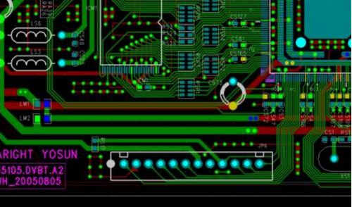
Before making a four-layer circuit board, you first need to design the circuit board. By using electronic design automation (EDA) software, you can draw circuit diagrams and layouts. Make sure that all electronic components can be connected correctly, and consider the requirements of signal transmission and power supply.
The second step is to draw the inner layer.
The four-layer circuit board has two inner layers, located between the top and bottom layers. Draw the required circuit connections on the inner layers, using conductive ink or copper clad film. These inner layers will provide signal transmission paths inside the circuit board.
The third step is to make outer layers.
Make outer layers on the top and bottom layers of the circuit board, which are usually used for layout and silk screen. The layout layer indicates where the electronic components are placed, and the silk screen layer is used to mark the component name or identifier for subsequent assembly and maintenance.
Four-layer circuit board production method, four-layer circuit board production process
The fourth step is chemical etching and gold plating. The manufactured circuit board is chemically etched to remove the unnecessary part of the copper layer. The gold plating can improve the conductivity and corrosion resistance of the circuit board.
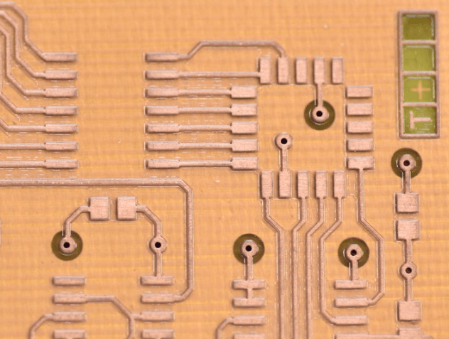
The fifth step is drilling and slotting.
Drill holes in the circuit board to install electronic components and connect circuits. Through slotting, the circuit board can be divided to meet specific application requirements.
The sixth step is welding components and assembly.
Using professional welding technology, electronic components are welded to the four-layer circuit board. Then assembly is carried out, including installing devices, plug-ins and connecting wires.
Four-layer circuit board production method, four-layer circuit board production process
The seventh step is testing and quality control.
After the production is completed, the four-layer circuit board is fully tested to confirm that it is functioning properly. Ensure that the quality of the circuit board meets the specified standards and requirements.
Through the above steps, you can successfully make a high-quality four-layer circuit board. But please note that making a four-layer circuit board requires certain professional knowledge and technology, and beginners are recommended to operate under the guidance of professionals.
Summary: This article introduces the production process and method of the four-layer circuit board. By understanding the design, layer drawing and processing steps of the circuit board, I hope that readers can better understand the key links in the electronic manufacturing process. Making a four-layer circuit board requires attention to quality control and testing to ensure that it functions properly. I hope this article is helpful to readers!

4-layer PCB production process:
1: Cutting process: large sheet → cutting according to MI requirements → brazing → beer fillet\edge grinding → board output, purpose: according to the requirements of the engineering data MI, on the large sheet that meets the requirements, cut into small pieces to produce boards. Small pieces of sheet that meet customer requirements.
2: Lamination process: adding an insulating layer between each layer and sticking each other firmly.
3: Drilling process: stacking pins → upper board → drilling → lower board → inspection\repair, purpose: according to the engineering data, on the sheet that meets the required size, drill the required hole diameter at the corresponding position.
4: Copper deposition process: rough grinding → hanging board → copper deposition automatic line → lower board → soaking % dilute H2SO4 → thickening copper, purpose: copper deposition is to use chemical methods to deposit a thin layer of copper on the insulating hole wall.
5: Graphic transfer process: (blue oil process): grinding board → printing the first side → drying → printing the second side → Drying → exposure → developing → inspection; (dry film process): hemp board → laminating → standing → alignment → exposure → standing → developing → inspection, purpose: graphic transfer is to transfer the image on the production film to the board.
6: Graphic electroplating process: upper board → degreasing → water washing twice → micro-etching → water washing → pickling → copper plating → water washing → acid dipping → tin plating → water washing → lower board, purpose: graphic electroplating is to electroplate a copper layer of required thickness and a gold-nickel or tin layer of required thickness on the exposed copper skin of the circuit pattern or on the hole wall.
7: Reduction Film process: Water film: insert the rack → alkali dip → rinse → scrub → pass the machine; Dry film: place the board → pass the machine, purpose: use NaOH solution to remove the anti-plating covering film layer to expose the non-circuit copper layer.
8: Solder mask process: grind the board → print photosensitive green oil → fix the board → expose → develop; grind the board → print the first side → bake the board → print the second side → bake the board, purpose: green oil is to transfer the pattern of green oil film to the board, which plays a role in protecting the circuit and preventing tin from the circuit when welding parts.
9: Character process: after the green oil is finally fixed → cool and stand Setting → Adjusting the screen → Printing characters → Post-fixing, Purpose: The characters are provided as a mark for easy identification.
10: Surface treatment (taking tin-spraying plate as an example) Process: Micro-etching → Air drying → Preheating → Rosin coating → Solder coating → Hot air leveling → Air cooling → Washing and air drying. Purpose: Plate a nickel\gold layer of the required thickness on the plug finger to make it more hard and wear-resistant. Purpose: Tin-spraying is to spray a layer of lead tin on the exposed copper surface not covered with solder resist to protect the copper surface from corrosion and oxidation to ensure good welding performance.
11: Molding, purpose: to punch out the shape required by the customer through die stamping or CNC punching machine. The molding methods include organic punching, beer board, hand punching, and hand cutting.
12: Testing process: upper mold → plate placement → test → qualified → FQC visual inspection → unqualified → repair → return to test → OK → REJ → scrap, purpose: to detect defects that affect functionality such as open circuits and short circuits that are not easily found visually through electronic 00% testing.
13: Final inspection process: incoming materials → check information → visual inspection → qualified → FQA spot check → qualified → packaging → unqualified → processing → inspection OK, purpose: to conduct 00% visual inspection of board appearance defects, and repair minor defects to avoid the outflow of problematic and defective boards.


