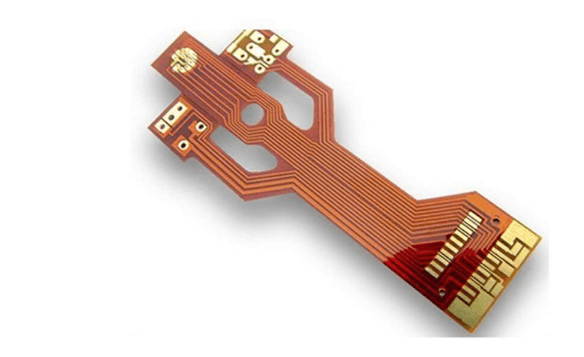
4 layer rigid flex pcb stackup
1.FPC multi-layer board folding and stacking design principles
Multilayer structure: FPC multilayer boards combine multiple conductive layers and insulating layers through lamination technology to form a complex three-dimensional circuit structure.
Folding design: Taking advantage of the flexible characteristics of FPC, the multi-layer board is folded to reduce the space occupied while maintaining circuit connectivity.
Stacking technology: Through precise alignment and fixing technology, multiple FPC layers are stacked together to achieve higher circuit density and performance.
2.Technical advantages of FPC multi-layer board folding and stacking design
Space optimization: The folding and stacking design significantly reduces the size of the circuit board, making it possible to miniaturize electronic devices.
Performance improvement: The multi-layer structure provides more wiring layers and signal transmission paths, improving the performance and reliability of the circuit.
Design flexibility: Designers can flexibly design folding and stacking FPC multi-layer boards according to the specific needs of the equipment.
3.Application of FPC multilayer board folding and stacking design in electronic equipment
Smartphones: In smartphones, the folding and stacking design of FPC multi-layer boards is widely used in camera modules, display connections, etc.
Wearable devices: The compact space and flexibility requirements of wearable devices make FPC multilayer board design an ideal choice.
Automotive electronics: In automotive electronic control systems, FPC multilayer board design helps achieve complex electronic system layout and signal transmission.
4.Challenges and solutions for folding and stacking design of FPC multi-layer board
Precise alignment: Ensuring precise alignment between layers during the stacking process is one of the key technical challenges.
Thermal Management: As circuit density increases, thermal management becomes an important factor to consider in design.
Material selection: Select appropriate flexible substrates and conductive materials to ensure the performance and durability of the FPC multilayer board.
The folding and stacking design of FPC multilayer boards is an important innovation in the field of electronic manufacturing. It provides an effective solution for the miniaturization and high performance of electronic equipment. With the continuous advancement of technology and the expansion of application fields, FPC multilayer board design will play a more important role in future electronic manufacturing.
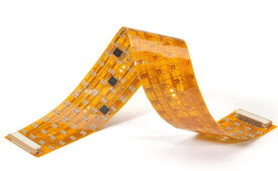
Characteristics of rigid-soft PCB stacking
- Fewer solder joints and connectors
The rigid-flexible stack features fewer solder joints and connectors than conventional printed circuit boards. This means it reduces the risk of soldering errors, which can lead to expensive rework of flexible PCB parts and even circuit failures.
- Minimum plate thickness
These rigid flexible plate technologies use thin films to achieve effective plate thickness reduction without compromising quality or reliability. The thickness of this board ranges from 0.2 mm to 0.4 mm, making it more durable.
- High thermal intensity
Rigid-flexible PCBs have better heat dissipation and higher reliability than typical rigid board environments.
- High aspect ratio
A high aspect ratio is when the width is greater than the height. It allows more space between each component on the circuit board, which helps in signal transmission. In addition, the high aspect ratio not only permits more space between the tracks, but also allows for easier routing of wires and other components.
Advantages of rigid-soft PCB stacking
Rigid and flexible design not only enable flexible circuit boards with 3D degrees of freedom, which is now the standard norm, but also have other benefits such as reduced maintenance and more uniform power distribution. Rigid and flexible printed circuit boards also facilitate optimized enclosure solutions.
- Better durability and flexibility
Flexibility and durability are key components of the PCB stack. The flexibility of the PCB stack also depends on the number of layers and data types used in the PCB.
The goal of rigid-flexible stacking of PCBs is to reduce the strain on the PCB that can cause damage to the circuit board. Rigid and flexible PCBs also have excellent mechanical performance, good dielectric performance and a wide operating temperature range, making them more durable.
- Save space
In rigid and flexible designs, space saving is one of the most important factors. Save space, reduce production costs, and stack rigid PCBs. Its thin and wide surface area allows the implementation of complex circuits without sacrificing the efficiency of the flexible circuit.
Rigid-flexible bonding is a way to enhance the overall structure of PCB boards through rigid-flexible bonding. The combination of rigidity and flexibility technology can effectively improve the bending stiffness and bending performance of the PCB board, making it more stable and reliable during operation.