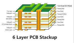
6-layer pcb stackup
Best Practices for 6-layer PCB Stackup Design.
When designing a 6-layer PCB stackup, following best practices is key to ensuring board performance and reliability.
First, a reasonable hierarchy is the foundation for success.
Typically, a 6-layer PCB stackup includes two signal layers, two power layers, and two ground layers. Such a configuration not only helps reduce electromagnetic interference (EMI), but also optimizes signal integrity.
Next, the layout of the signal layer is critical.
To minimize signal interference, it is recommended that high-speed signals be placed on the inner layer, while low-speed signals can be placed on the outer layer. This arrangement helps protect high-speed signals from external noise. In addition, signal layers should be avoided as much as possible to reduce crosstalk.
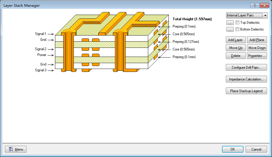
In the design of the power layer and ground layer, it is critical to ensure good power distribution and grounding.
The power layer should be as close to the ground layer as possible to form an effective decoupling capacitor, thereby reducing power noise. In this way, the stability of the power supply and the overall performance of the circuit can be improved. At the same time, the ground layer should be kept intact as much as possible, avoiding unnecessary cutting and segmentation to ensure a good ground path.
In addition, the use of vias is also an important consideration in the design.
The number and location of vias should be carefully planned to avoid interference with the signal path. Too many vias may cause signal reflection and loss, so unnecessary vias should be minimized. At the same time, the size and shape of the vias should also meet the design specifications to ensure signal integrity.
In the design process, thermal management is also an aspect that cannot be ignored. 6-layer PCBs are usually used for high-density and high-performance applications, so heat management is particularly important. Through reasonable layout and the use of thermal vias, heat can be effectively conducted away from high-power components to prevent overheating.
Finally, design verification and testing are key steps to ensure the success of 6-layer PCB stacking design. After completing the design, comprehensive simulation and testing are carried out to verify the performance and reliability of the circuit board. In this way, potential problems can be discovered and solved in time to ensure the quality of the final product.
In short, the best practices for 6-layer PCB stacking design include reasonable hierarchy, optimized signal layer layout, good power and grounding design, appropriate use of vias, and effective thermal management. By following these best practices, the performance and reliability of the circuit board can be significantly improved to meet the needs of high-performance applications.


