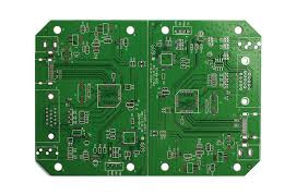
1 layer pcb
1.What is 1-layer pcb
1-layer PCB, or single-layer printed circuit board, is the most basic type of circuit board in electronic devices. It consists of a layer of conductive material (usually copper) and an insulating substrate. The design of a single-layer PCB is relatively simple and is suitable for low-complexity circuits and cost-sensitive applications. Despite its simple structure, 1-layer PCB still plays an important role in the design and manufacture of electronic products.
2.What is the structural composition of a 1-layer PCB?
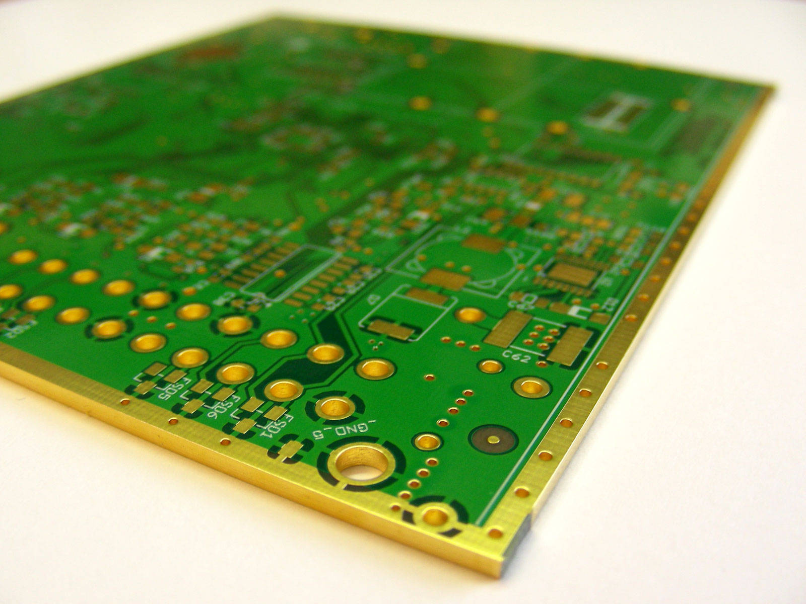
The substrate of a single-layer PCB is usually made of insulating materials, the most common of which is glass fiber reinforced epoxy resin, commonly known as FR-4. This material has excellent mechanical strength and electrical insulation properties and can remain stable under various environmental conditions.
In addition, FR-4 material also has good heat resistance and chemical corrosion resistance, which makes it widely used in electronic devices.
In addition to FR-4, other common substrates include phenolic resin paper-based materials (FR-1, FR-2) and composite materials (CEM-1, CEM-3), each of which has its own advantages and disadvantages and is suitable for different application scenarios.
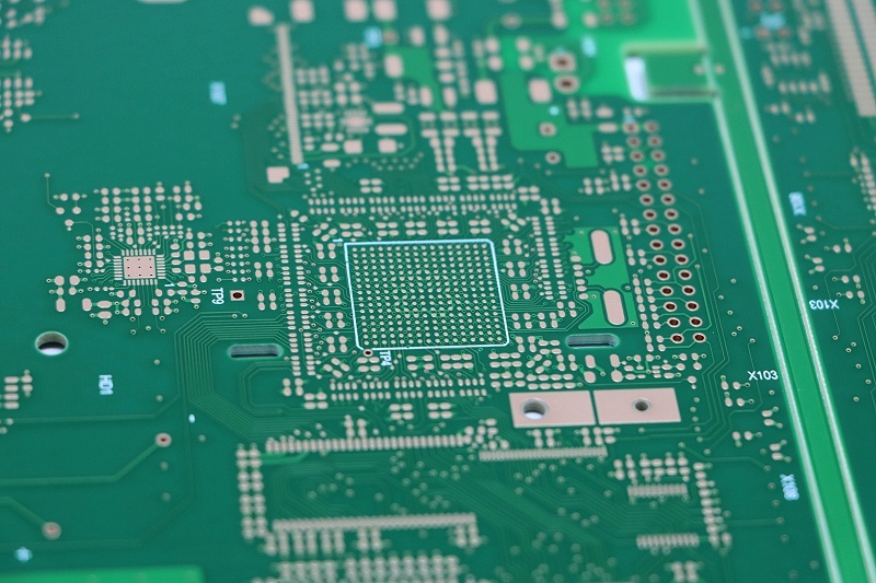
Next, the conductive layer of a single-layer PCB is usually composed of copper foil. The thickness of the copper foil is generally between 18 microns and 70 microns, and the specific choice depends on the current carrying capacity and heat dissipation requirements of the circuit.
The copper foil is attached to the substrate through chemical deposition or electroplating processes to form a conductive path. In order to protect the copper foil and prevent oxidation, a layer of solder or other protective coating is usually covered on its surface.
In addition, the design and layout of the conductive layer have an important impact on the performance of the circuit. Reasonable layout can reduce electromagnetic interference and signal loss and improve the reliability of the circuit.
GET PCB MANUFACTURING AND ASSEMBLY QUOTE NOW!
3.What are the advantages of 1-layer PCB?
(1)low manufacturing cost
(2)the design and manufacturing cycle of single-layer PCB is shorter
(3)has higher reliability
(4)reducing the possibility of electrical failure
(5) simple structure and more intuitive fault location and repair processes.
4.What are the disadvantages of 1-layer PCB?
(1)the flexibility of circuit design is limited, and it is difficult to realize complex circuit functions.
(2)the single-layer structure makes the signal transmission path longer, which may cause signal delay and interference problems.
First, the design process of a 1-layer PCB includes several key steps. Designers need to use electronic design automation (EDA) software to create a circuit diagram and convert it into a PCB layout.
The layout design needs to consider factors such as component placement, wire routing, and electrical performance.
Since there is only one layer of conductive material, designers must pay special attention to avoid wire crossing and signal interference. This simplification of design makes 1-layer PCBs widely used in small electronic devices such as calculators, remote controls, and simple sensor modules.
Next, the manufacturing process of a 1-layer PCB is also relatively simple. First, copper foil is laminated onto an insulating substrate, and then the unwanted copper is removed through a photolithography or etching process to form the desired circuit pattern.
Next, drilling and electroplating are performed to allow the electronic components to be mounted. Finally, the components are fixed to the PCB by soldering. Due to the simple process, 1-layer PCB has low production cost and is suitable for mass production.
However, 1-layer PCB also has its limitations. Since there is only one layer of conductive material, the flexibility of circuit design is limited, and it is difficult to realize complex circuit functions. In addition, the single-layer structure makes the signal transmission path longer, which may cause signal delay and interference problems.
Therefore, in applications that require high performance and high-density circuits, designers usually choose multi-layer PCBs.
Nevertheless, 1-layer PCB still has irreplaceable advantages in many applications. Its low cost and easy manufacturing characteristics make it the first choice for many start-ups and small electronic projects.
In addition, the simplicity of single-layer PCB also makes it widely used in education and training, helping students and beginners to quickly master the basic concepts of circuit design.
In short, as the most basic type of circuit board, 1-layer PCB, although limited in complexity and performance, its advantages in cost, manufacturing and education make it occupy an important position in the electronics industry.
Through reasonable design and application, 1-layer PCB can meet the needs of many low-complexity electronic devices and provide a solid foundation for the diversified development of electronic products.
GET PCB AND ASSEMBLY SERVICE QUOTE NOW!
5.Application of 1-layer PCB
(1)various types of consumer electronics,
(2)simple electronic devices such as remote controls, calculators, and electronic toys
(3)used in portable devices such as smartphones and tablets.
the application of single-layer PCB in consumer electronics is also reflected in its wide applicability. Single-layer PCBs are suitable for various types of consumer electronics, from simple household appliances to complex portable devices.
For example, simple electronic devices such as remote controls, calculators, and electronic toys usually use single-layer PCBs because the circuits of these devices are relatively simple and do not require the complex structure of multi-layer PCBs.
On the other hand, single-layer PCBs are also widely used in portable devices such as smartphones and tablets. Although the circuit design of these devices is relatively complex, single-layer PCBs can still meet their functional requirements through reasonable design and optimization.
In addition, single-layer PCB also has certain advantages in terms of environmental protection. Because its manufacturing process is relatively simple, it requires less material and energy consumption, thus reducing its impact on the environment.
With the continuous improvement of environmental awareness, more and more electronic product manufacturers are beginning to pay attention to the environmental performance of their products, and single-layer PCBs are favored for their environmental properties.
In summary, the wide application of single-layer PCBs in consumer electronics is not only due to its cost-effectiveness and design convenience, but also its wide applicability and environmental protection advantages.
With the continuous advancement of science and technology and changes in market demand, the application prospects of single-layer PCB in consumer electronic products will be broader.
By continuously optimizing the design and manufacturing process, single-layer PCBs will continue to play an important role in consumer electronics, bringing more high-quality, low-cost electronic products to consumers.