HDI circuit boards
1.What is HDI circuit boards
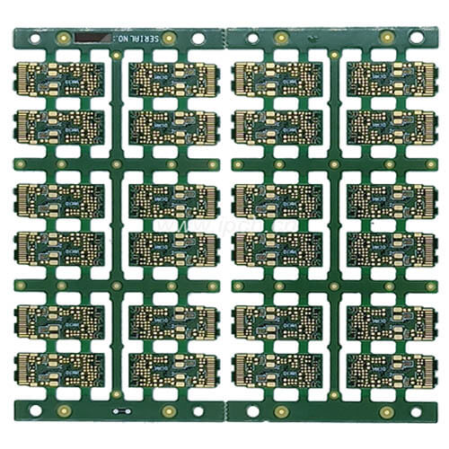
HDI (High Density Interconnector) board, or high-density interconnect board, is a circuit board with a relatively high line distribution density that uses micro blind buried hole technology. It contains inner and outer layer circuits, and then uses drilling and metallization processes in the holes to achieve the connection function between the internal layers of each layer of circuits. As electronic products develop towards high density and high precision, the same requirements are put forward for circuit boards. The most effective way to increase the density of PCBs is to reduce the number of through holes and accurately set blind holes and buried holes to achieve this requirement, which gave rise to HDI boards.
2.What is the material composition of a HDI circuit boards?
the substrate of HDI circuit boards usually adopts FR-4, which is an epoxy resin material reinforced by glass fiber. FR-4 material has excellent mechanical strength and electrical insulation properties, and can remain stable in high-temperature environments.
However, with the continuous miniaturization and high-performance of electronic devices, the limitations of FR-4 materials have gradually emerged, especially in high-frequency applications, where its dielectric constant and loss factor are high, which may affect the quality of signal transmission.
To overcome these problems, other high-performance materials are also used in HDI circuit boards. For example, polyimide (PI) material has become an important choice due to its excellent heat resistance and electrical properties.
PI material is not only stable in high-temperature environments, but also has a low dielectric constant and loss factor, which is suitable for high-frequency signal transmission. In addition, liquid crystal polymer (LCP) material has also gradually attracted attention.
LCP material has extremely low dielectric constant and loss factor, and performs well in high-frequency applications, suitable for 5G communication equipment and high-frequency radar systems.
In addition to the substrate, the conductive material of HDI circuit boards is also crucial. Traditional copper foil is still the main conductive material due to its excellent conductivity and processability.
However, in order to further improve the performance of circuit boards, some new conductive materials have emerged in recent years. For example, graphene has become a potential alternative material due to its ultra-high conductivity and mechanical strength. Although the application of graphene is still in the research stage, it has broad application prospects in future HDI circuit boards.
In addition, a variety of auxiliary materials are involved in the manufacturing process of HDI circuit boards, such as drilling filling materials and surface treatment materials.
Drilling filling materials usually use epoxy resin or conductive silver paste to ensure the filling and conductivity of micropores. Surface treatment materials include gold plating, silver plating and organic antioxidants (OSP) to improve the anti-oxidation performance and welding reliability of circuit boards.

GET PCB MANUFACTURING AND ASSEMBLY QUOTE NOW!
3.What are the advantages of HDI circuit boards ?
(1)high-density nature.
(2)higher signal transmission speeds and better signal integrity.
4.What are the disadvantages of 10-layer PCB?
(1)higher cost
(2)face a higher risk of failure in practical applications.
HDI circuit boards also feature higher signal transmission speeds and better signal integrity. Due to the use of shorter signal paths and smaller capacitive and inductive effects in its design, HDI circuit boards can effectively reduce signal delays and interference.
This is especially important for high-speed data transmission and high-frequency applications, such as 5G communication equipment and high-speed computer systems. Therefore, HDI circuit boards have broad application prospects in these fields.
However, HDI circuit boards also have some disadvantages. First, its manufacturing cost is higher. Since the design and manufacturing process of HDI circuit boards is complex and requires the use of advanced processes and equipment, its production cost is significantly higher than that of traditional circuit boards. For some cost-sensitive applications, this can become a limiting factor.
In addition, the manufacturing process of HDI circuit boards has high technical requirements and requires engineers with professional knowledge and experience for design and production. This increases manufacturing difficulty and time costs, which may affect the time to market of the product.
Another drawback to be aware of is the reliability of HDI circuit boards. Although HDI circuit boards offer many advantages in design, their microvia and fine line structures may face a higher risk of failure in practical applications.
For example, the filling and connection quality of microvias can affect the overall performance and longevity of a circuit board. Therefore, when using HDI circuit boards, special attention needs to be paid to their manufacturing quality and testing process to ensure their reliability.
To sum up, HDI circuit boards have significant advantages in high-density design, high-speed signal transmission and miniaturization applications, but their high manufacturing costs, technical requirements and reliability issues cannot be ignored. When choosing whether to use an HDI circuit board, these advantages and disadvantages need to be considered to ensure optimal performance and cost-effectiveness in a specific application. By continuously improving the manufacturing process and technical level, the application prospects of HDI circuit boards will be broader, bringing great benefits to the electronics manufacturing industry.
GET PCB AND ASSEMBLY SERVICE QUOTE NOW!
5.Application of HDI circuit boards
(1)In the field of smartphones
(2)tablets and laptops
(3)in wearable devices
(4)in smart home devices
The application of HDI circuit boards in consumer electronics has become more and more common. First of all, HDI circuit board, that is, high-density interconnect circuit board, has become one of the core components of modern consumer electronics products due to its high density and high performance.
With the advancement of technology and consumers’ increasing performance requirements for electronic products, the application scope of HDI circuit boards is also expanding.
In the field of smartphones, the application of HDI circuit boards is particularly significant. As an indispensable device in modern people’s lives, smartphones require a high degree of integration and miniaturization in their internal structures.
HDI circuit boards are able to achieve more functions in a limited space through their multi-layer design and tiny via technology. This not only improves the performance of the smartphone but also makes its design thinner, lighter and more portable. In addition, the high reliability and high signal transmission speed of HDI circuit boards also ensure the stability and smoothness of smartphones under high-frequency use.
In addition to smartphones, tablets and laptops are also important application scenarios for HDI circuit boards. As people’s demand for mobile work and entertainment increases, these devices need to have higher processing power and longer battery life.
HDI circuit boards are able to meet these needs through their efficient circuit design and excellent heat dissipation performance. Not only can they support higher processing speeds, they can also effectively reduce power consumption, thereby extending the life of the device.
In addition, the application of HDI circuit boards in wearable devices cannot be ignored. Wearable devices such as smart watches and fitness trackers need to integrate multiple functions in a very small space, such as heart rate monitoring, GPS positioning and wireless communications.
The high-density design of the HDI circuit board makes the integration of these functions possible while ensuring the device’s portability and comfort. More importantly, the high reliability and durability of HDI circuit boards ensure the normal operation of wearable devices in various environments.
Looking further, the application of HDI circuit boards in smart home devices is also gradually increasing. Devices such as smart speakers, smart light bulbs, and smart door locks require efficient communication capabilities and stable performance.
Through its high-density interconnection technology, HDI circuit boards enable fast communication and data transmission between devices, thereby improving the overall performance and user experience of the smart home system.
To sum up, the application scenarios of HDI circuit boards in consumer electronics products are extensive and diverse. Whether it is smartphones, tablets, laptops, wearable devices and smart home devices, HDI circuit boards play a vital role.
With the continuous advancement of technology and the changing needs of consumers, the application prospects of HDI circuit boards will be broader. Through continuous innovation and optimization, HDI circuit boards will continue to promote the development of consumer electronics products and bring more convenience and surprises to people’s lives.
