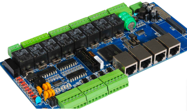
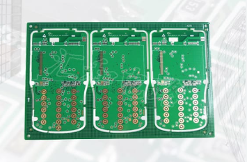
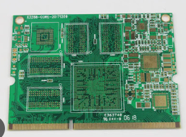
6 layer pcb prototype
It is crucial to understand the key steps and precautions when designing a 6 layer PCB prototype
First, the designer needs to clarify the functions and requirements of the circuit board.
This includes determining the basic parameters such as the size, number of layers, materials, and electrical performance of the circuit board. Through a detailed demand analysis, it is possible to ensure that the direction and goals of the design are clear, thereby avoiding major deviations in the subsequent design process.
Next, the designer should draw the circuit schematic.
This step is the basis of the entire design process, and all electrical connections and component layouts will be reflected in the schematic. In order to ensure the reliability and stability of the circuit, the designer needs to carefully check the parameters of each connection point and component to avoid problems such as short circuits and open circuits. In addition, reasonable component layout and electrical connections can effectively reduce electromagnetic interference and improve the overall performance of the circuit.
After completing the schematic design, the designer needs to design the PCB layout
. For a 6-layer PCB, a reasonable stacking structure is the key. Generally, the stacking structure of a 6-layer PCB includes two signal layers, two power layers, and two ground layers. Through a reasonable stacking structure, signal interference and power noise can be effectively reduced, and the stability and reliability of the circuit can be improved. 、
During the layout process, designers need to pay attention to the length and routing of signal lines to avoid signal lines that are too long or too complicated, thereby reducing signal delays and losses.
In addition, designers also need to plan power supply and grounding.
For multi-layer PCBs, the design of power supply and grounding is particularly important. Reasonable power supply and grounding planning can effectively reduce power supply noise and electromagnetic interference and improve the overall performance of the circuit. When planning power supply and grounding, designers need to ensure the integrity of the power supply and grounding layers to avoid breaks or discontinuities.
After completing the PCB layout design, designers need to perform simulation and verification.
Through simulation software, the performance of the circuit can be estimated and verified, and potential problems can be discovered and solved. Simulation and verification are key steps to ensure the correctness and reliability of circuit design. Designers need to carefully check every detail to ensure that the circuit can work properly in actual applications.
Finally, designers need to manufacture and test PCBs. When selecting a manufacturer,
designers need to consider the manufacturer’s technical capabilities and production quality to ensure that the manufacturing quality of the PCB meets the design requirements.
After manufacturing is completed, designers need to conduct comprehensive testing of the PCB to verify its electrical performance and functions to ensure that it can meet the expected design goals.
In summary, 6 layer PCB prototype design is a complex and delicate process, and designers need to maintain a high degree of meticulousness and rigor in every step. Through clear requirements, reasonable layout, precise simulation and rigorous testing, the final PCB prototype can be ensured to have excellent performance and reliability.
In the design and development process of IoT devices, the application of 6-layer PCB prototypes is particularly important.
First of all, IoT devices usually need to integrate multiple functional modules, such as sensors, communication modules, and processing units. The complexity and diversity of these modules require the circuit board to have a higher number of layers to support the transmission and processing of multiple signals. The 6-layer PCB prototype can provide enough wiring layers, allowing designers to arrange the circuit layout more flexibly, thereby improving the performance and reliability of the device.
In addition, the application of 6-layer PCB prototypes in IoT devices can also effectively reduce electromagnetic interference. IoT devices usually need to work in a complex electromagnetic environment, and electromagnetic interference may affect the normal operation of the device. By increasing the number of layers of the PCB, the signal isolation and shielding can be better achieved, thereby reducing the impact of electromagnetic interference. Specifically, the 6-layer PCB usually includes two signal layers, two power layers, and two ground layers. This structure can effectively reduce interference between signals and improve the stability of signal transmission.
Further, the application of 6-layer PCB prototypes in IoT devices can also improve the heat dissipation performance of the circuit. IoT devices generate a lot of heat during operation. If the heat is not dissipated in time, it may cause the device to overheat and affect its normal operation.
By increasing the number of layers, the 6-layer PCB prototype can better disperse heat and reduce the temperature of the circuit board, thereby improving the reliability and service life of the device.
At the same time, the 6-layer PCB prototype can also support higher integration and miniaturization design. IoT devices usually need to have the characteristics of miniaturization and high integration for easy installation and use. By increasing the number of layers, the 6-layer PCB prototype can integrate more functional modules in a limited space, thereby realizing the miniaturization design of the device.
This is of great significance for IoT devices that need to be installed in a small space, such as smart home devices, wearable devices, etc.
Finally, the application of 6-layer PCB prototypes in IoT devices can also speed up the product development cycle. In the development process of IoT devices, prototype design and testing are essential links.
By using 6-layer PCB prototypes, designers can design and debug circuits more quickly, thereby shortening the product development cycle and increasing the speed of product listing. This is of great strategic significance for the highly competitive IoT market.
In summary, the application of 6-layer PCB prototypes in IoT devices has many advantages, including improving circuit performance, reducing electromagnetic interference, enhancing heat dissipation performance, supporting miniaturization design, and accelerating product development cycle.
These advantages make 6-layer PCB prototypes an indispensable and important tool in the design and development process of IoT devices.