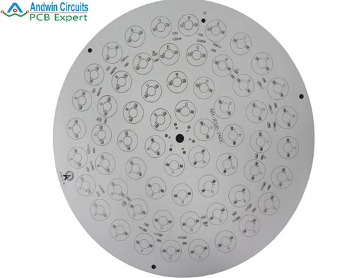
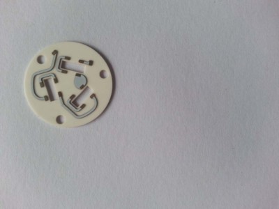
Ceramic pcb laminates
Advantages Of Ceramic PCB Laminates In High-Frequency Applications
When it comes to high-frequency applications, the choice of materials can make or break the performance of your electronic devices. One material that has been gaining traction in this field is ceramic PCB laminates. These laminates offer a plethora of advantages that make them particularly well-suited for high-frequency applications, and today, we’re going to dive into why that is.
First off, let’s talk about thermal management.
High-frequency applications often generate a significant amount of heat, and managing this heat is crucial for maintaining performance and longevity. Ceramic PCB laminates excel in this area due to their excellent thermal conductivity. Unlike traditional FR4 materials, ceramics can efficiently dissipate heat, reducing the risk of overheating and ensuring that your components stay cool even under heavy loads. This is particularly beneficial for applications like RF amplifiers and microwave circuits, where thermal management is a constant challenge.
Another key advantage of ceramic PCB laminates is their low dielectric constant and low loss tangent.
In high-frequency applications, signal integrity is paramount. The dielectric constant of a material affects the speed at which signals can travel through it, while the loss tangent measures how much signal is lost as it passes through the material. Ceramic laminates typically have a low dielectric constant and low loss tangent, which means they can transmit signals more efficiently and with less distortion. This results in clearer, more reliable signal transmission, which is essential for applications like satellite communications and radar systems.
Moreover, ceramic PCB laminates are incredibly durable.
They are resistant to a wide range of environmental factors, including moisture, chemicals, and extreme temperatures. This makes them ideal for use in harsh environments where other materials might fail. For instance, in aerospace and military applications, where conditions can be unpredictable and demanding, the robustness of ceramic laminates ensures that the electronic components remain functional and reliable.
In addition to their durability, ceramic PCB laminates also offer excellent mechanical stability.
They are less prone to warping and deformation compared to other materials, which is crucial for maintaining the integrity of high-frequency circuits. This stability ensures that the components remain in place and that the connections stay secure, even under mechanical stress. This is particularly important in applications like automotive radar systems, where vibrations and mechanical shocks are common.
Furthermore, ceramic PCB laminates are highly customizable.
They can be manufactured in various thicknesses and configurations to meet the specific needs of different applications. This flexibility allows designers to optimize the performance of their circuits by choosing the right laminate for their particular requirements. Whether you need a thin, lightweight laminate for a compact device or a thicker, more robust one for a high-power application, ceramics can be tailored to fit the bill.
Lastly, let’s not forget about the cost-effectiveness of ceramic PCB laminates.
While they may be more expensive upfront compared to traditional materials, their long-term benefits often outweigh the initial investment. The improved performance, reliability, and durability of ceramic laminates can lead to lower maintenance costs and fewer replacements over time, making them a cost-effective choice in the long run.
In conclusion, ceramic PCB laminates offer a range of advantages that make them ideal for high-frequency applications. From superior thermal management and signal integrity to durability and mechanical stability, these laminates provide the performance and reliability needed to meet the demands of modern electronic devices. So, if you’re working on a high-frequency project, it might be worth considering ceramic PCB laminates as your material of choice.
Thermal Management Solutions Using Ceramic PCB Laminates
When it comes to thermal management solutions in the world of electronics, ceramic PCB laminates are quickly becoming the go-to material for engineers and designers alike.
These laminates are not just a passing trend; they offer a range of benefits that make them ideal for high-performance applications. So, what exactly makes ceramic PCB laminates so special, and why should you consider them for your next project?
First off, let’s talk about heat. In the realm of electronics, managing heat is crucial.
Excessive heat can lead to reduced performance, shorter lifespans, and even catastrophic failures. Traditional materials like FR4 just don’t cut it when it comes to high-power applications.
This is where ceramic PCB laminates come into play. They have excellent thermal conductivity, which means they can efficiently dissipate heat away from critical components. This is particularly important in applications like power electronics, LED lighting, and RF modules, where heat management is a constant challenge.
Moreover, ceramic PCB laminates are incredibly durable.
Unlike their traditional counterparts, they can withstand higher temperatures without degrading. This makes them perfect for harsh environments where reliability is key. Imagine a scenario where your device is exposed to extreme temperatures, whether it’s in an industrial setting or even in outer space. Ceramic laminates can handle it, ensuring that your device continues to function optimally.
Another advantage of ceramic PCB laminates is their electrical insulation properties.
They offer high dielectric strength, which means they can prevent electrical breakdowns even at high voltages. This is a game-changer for applications that require both high thermal conductivity and electrical insulation. For instance, in power modules, you need a material that can handle high currents without causing short circuits. Ceramic laminates fit the bill perfectly.
Transitioning to the manufacturing side of things, ceramic PCB laminates are also relatively easy to work with.
They can be processed using standard PCB manufacturing techniques, which means you don’t have to invest in specialized equipment. This makes them a cost-effective solution for many applications. Plus, they are compatible with various types of surface finishes, so you have the flexibility to choose the best option for your specific needs.
Now, you might be wondering about the environmental impact.
The good news is that ceramic PCB laminates are generally more eco-friendly compared to traditional materials. They are often made from naturally occurring minerals and can be recycled more easily. This is a significant advantage in today’s world, where sustainability is becoming increasingly important.
In terms of design flexibility, ceramic PCB laminates offer a lot of room for innovation.
They can be used in multi-layer designs, allowing for more complex and compact circuits. This is particularly useful in applications where space is at a premium, such as in medical devices or wearable technology. The ability to create intricate designs without compromising on performance is a huge plus.
So, if you’re looking for a thermal management solution that offers excellent performance, durability, and flexibility, ceramic PCB laminates are definitely worth considering. They bring a host of benefits to the table, making them an ideal choice for a wide range of applications. Whether you’re dealing with high-power electronics, harsh environments, or complex designs, ceramic laminates have got you covered. Give them a try, and you might just find that they are the missing piece in your thermal management puzzle.
Comparing Ceramic PCB Laminates To Traditional FR4 Materials
When it comes to printed circuit boards (PCBs), the choice of material can make a world of difference in performance, durability, and overall efficiency. While traditional FR4 materials have long been the go-to for many applications, ceramic PCB laminates are increasingly gaining traction. So, what sets these two apart, and why might you consider making the switch to ceramic?
First off, let’s talk about thermal conductivity.
FR4, which is essentially a woven glass-reinforced epoxy laminate, has decent thermal properties but can struggle under high-temperature conditions. This is where ceramic PCB laminates shine. Ceramics, such as aluminum oxide or aluminum nitride, offer superior thermal conductivity, which means they can dissipate heat much more effectively. This is particularly beneficial for high-power applications or environments where heat management is crucial. Imagine working on a high-frequency RF application or a power LED circuit; the last thing you want is for your board to overheat and fail. Ceramic laminates can handle these conditions with ease, providing a more reliable and long-lasting solution.
Moving on to mechanical strength, FR4 is pretty robust but can be somewhat brittle, especially when subjected to mechanical stress or vibration.
Ceramic laminates, on the other hand, are incredibly strong and resistant to wear and tear. This makes them ideal for applications that require a high degree of mechanical stability, such as aerospace or automotive industries. Picture a scenario where your PCB is part of a critical system in an aircraft; the mechanical reliability of ceramic laminates can offer peace of mind that FR4 simply can’t match.
Another point to consider is the dielectric properties.
FR4 has a relatively high dielectric constant, which can be a limiting factor in high-frequency applications. Ceramic materials generally have a lower dielectric constant, which translates to better performance in high-frequency circuits. This makes ceramic laminates a preferred choice for RF and microwave applications. If you’re working on a project that involves high-speed data transmission, the lower dielectric loss of ceramic materials can significantly enhance signal integrity.
Cost is often a major factor in material selection, and here, FR4 has traditionally held the upper hand.
It’s widely available and relatively inexpensive, making it a popular choice for many standard applications. However, the gap is narrowing as ceramic manufacturing processes become more efficient and cost-effective. While ceramic laminates may still come at a premium, the long-term benefits in terms of performance and reliability can often justify the initial investment. Think of it as paying a bit more upfront for a product that will save you money and headaches down the line.
Lastly, let’s not forget about environmental considerations.
FR4 materials are not particularly eco-friendly, given that they are based on epoxy resins and glass fibers. Ceramics, being more natural and less chemically intensive, offer a greener alternative. In an age where sustainability is becoming increasingly important, this could be another compelling reason to consider ceramic PCB laminates.
In summary, while traditional FR4 materials have their merits and will likely remain in use for many standard applications, ceramic PCB laminates offer several advantages that make them worth considering. From superior thermal and mechanical properties to better dielectric performance and environmental benefits, ceramics are proving to be a formidable contender in the world of PCB materials. So, the next time you’re faced with a choice, it might be worth giving ceramic laminates a closer look.
Innovations In Ceramic PCB Laminate Manufacturing Techniques
Ceramic PCB laminates have been making waves in the electronics industry, and for good reason. These materials offer a unique blend of thermal stability, electrical insulation, and mechanical strength, making them ideal for high-performance applications. But what’s really exciting is the recent surge in innovative manufacturing techniques that are pushing the boundaries of what ceramic PCB laminates can do.
One of the most intriguing advancements is the use of additive manufacturing, or 3D printing, in the production of ceramic PCBs.
Traditional methods often involve complex, multi-step processes that can be time-consuming and costly. However, 3D printing allows for the creation of intricate designs with a level of precision that was previously unattainable. This not only speeds up the production process but also opens up new possibilities for custom designs and rapid prototyping. Imagine being able to print a fully functional ceramic PCB in a matter of hours rather than days or weeks. It’s a game-changer.
Another noteworthy development is the integration of nanotechnology into ceramic PCB laminates.
By incorporating nanoparticles into the ceramic matrix, manufacturers can significantly enhance the material’s properties. For instance, adding silver nanoparticles can improve electrical conductivity, while silicon carbide nanoparticles can boost thermal conductivity. This means that ceramic PCBs can now handle even higher power densities and more extreme operating conditions, making them perfect for cutting-edge applications like electric vehicles and advanced aerospace systems.
Moreover, the advent of laser machining techniques has revolutionized the way ceramic PCBs are fabricated.
Lasers can cut and shape ceramic materials with incredible precision, allowing for the creation of complex geometries that were once thought impossible. This is particularly beneficial for applications that require miniaturization, such as medical devices and wearable technology. With laser machining, manufacturers can produce smaller, more efficient ceramic PCBs without sacrificing performance.
In addition to these high-tech methods, there’s also been a resurgence in interest in traditional techniques like tape casting and screen printing, albeit with modern twists.
Tape casting involves spreading a ceramic slurry onto a flat surface to create thin, flexible sheets that can be layered and laminated. Recent improvements in slurry formulations and casting techniques have resulted in higher-quality laminates with fewer defects. Similarly, screen printing has been refined to allow for finer resolution and better control over the deposition of conductive inks, making it easier to create intricate circuit patterns on ceramic substrates.
What’s particularly exciting is how these innovations are being combined to create hybrid manufacturing processes.
For example, a manufacturer might use 3D printing to create a complex ceramic structure, then employ laser machining to fine-tune the details, and finally apply screen printing to add the necessary circuitry. This multi-faceted approach allows for unprecedented levels of customization and performance optimization.
As we look to the future, it’s clear that the landscape of ceramic PCB laminate manufacturing is rapidly evolving. These innovations are not just incremental improvements; they represent a fundamental shift in how we think about and produce these critical components. Whether it’s through the precision of 3D printing, the enhanced properties provided by nanotechnology, or the versatility of laser machining, the possibilities are virtually limitless. So, the next time you marvel at the performance of your high-tech gadgets, remember that behind the scenes, ceramic PCB laminates and the cutting-edge techniques used to create them are playing a crucial role in making it all possible.