Ceramic pcb manufacturing process
Introduction To Ceramic PCB Manufacturing
If you’ve ever wondered how the tech behind your gadgets stays cool and efficient, you might want to take a closer look at ceramic PCBs. These little wonders are the unsung heroes in the world of electronics, especially when it comes to high-power applications. So, let’s dive into the fascinating process of ceramic PCB manufacturing and see what makes them so special.
First off, what exactly is a ceramic PCB?
Unlike traditional PCBs made from fiberglass or other materials, ceramic PCBs use a ceramic base. This gives them excellent thermal conductivity and electrical insulation properties, making them ideal for high-frequency and high-temperature applications. Think of them as the cool kids in the PCB world, quite literally.
The journey of a ceramic PCB starts with the selection of the ceramic material.
Common choices include alumina (Al2O3), aluminum nitride (AlN), and beryllium oxide (BeO). Each of these materials has its own set of advantages, but alumina is the most widely used due to its cost-effectiveness and good thermal properties. Once the material is chosen, it’s time to move on to the next step: substrate preparation.
Substrate preparation involves cleaning and sometimes polishing the ceramic material to ensure a smooth surface.
This is crucial because any imperfections can affect the performance of the final product. After the substrate is prepped, it’s time for the fun part: applying the conductive layers.
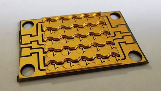
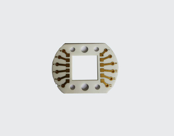
Conductive layers are usually made of metals like copper, silver, or gold.
These metals are applied to the ceramic substrate using various methods such as screen printing, sputtering, or electroplating. Screen printing is the most common method and involves using a stencil to apply a paste made of metal particles and a binding agent. Once the paste is applied, the substrate is heated to remove the binding agent and fuse the metal particles together, forming a solid conductive layer.
Now that we have our conductive layers in place, it’s time to create the circuit pattern.
This is done using a process called photolithography. In simple terms, photolithography involves coating the substrate with a light-sensitive material called photoresist. A mask with the desired circuit pattern is then placed over the substrate, and the whole setup is exposed to ultraviolet light. The light hardens the photoresist in the exposed areas, leaving the unexposed areas soft. These soft areas are then washed away, revealing the underlying metal, which can be etched away to create the circuit pattern.
After the circuit pattern is etched, the next step is to add any additional layers or components.
This could involve adding more conductive layers, insulating layers, or even embedding passive components like resistors and capacitors directly into the PCB. Each additional layer goes through a similar process of deposition, patterning, and etching.
Finally, the ceramic PCB undergoes a series of tests to ensure it meets all the required specifications.
These tests can include electrical testing, thermal cycling, and even X-ray inspection to check for any hidden defects. Once the PCB passes all these tests, it’s ready to be shipped off and used in everything from LED lighting to aerospace applications.
So there you have it, a behind-the-scenes look at the ceramic PCB manufacturing process. It’s a complex and meticulous journey, but the end result is a high-performance, reliable PCB that can handle the toughest conditions. Next time you marvel at the efficiency of your high-tech gadgets, you’ll know a little more about the incredible technology that makes it all possible.
Key Steps In Ceramic PCB Fabrication
Ceramic PCB manufacturing is a fascinating process that combines advanced technology with meticulous craftsmanship. If you’ve ever wondered how these high-performance circuit boards come to life, you’re in for a treat. Let’s dive into the key steps involved in fabricating ceramic PCBs, and you’ll see just how intricate and rewarding this process can be.
First off, it all begins with the selection of the ceramic substrate.
This is a crucial step because the substrate forms the foundation of the PCB. Typically, materials like alumina, aluminum nitride, or beryllium oxide are chosen for their excellent thermal conductivity and electrical insulation properties. Once the substrate is selected, it is cut into the desired shape and size, setting the stage for the subsequent steps.
Next, we move on to the cleaning process.
The ceramic substrate must be meticulously cleaned to remove any contaminants that could interfere with the adhesion of the conductive layers. This is usually done using a combination of ultrasonic cleaning and chemical treatments. Think of it as giving the substrate a spa day to ensure it’s in perfect condition for the next steps.
Following the cleaning, the substrate undergoes a process called screen printing.
This is where the magic starts to happen. A conductive paste, often made of silver, gold, or copper, is applied to the substrate through a stencil or screen. This paste forms the circuit patterns that will eventually carry electrical signals. The precision of this step is paramount, as any errors can lead to faulty circuits down the line.
Once the conductive paste is applied, the substrate is subjected to a drying process to remove any solvents from the paste.
This is typically done in a controlled environment to ensure uniform drying. After drying, the substrate is fired in a high-temperature furnace. This firing process, also known as sintering, causes the conductive particles in the paste to fuse together, forming a solid and durable conductive layer. It’s like baking a cake, but instead of a delicious treat, you get a robust circuit board.
After sintering, the next step is to apply a dielectric layer if needed.
This layer serves as an insulator between different conductive layers, allowing for multi-layered PCB designs. The dielectric material is applied using a similar screen-printing process and then cured to form a solid layer. This step can be repeated multiple times to build up the desired number of layers.
With the dielectric layers in place, the PCB is almost ready, but not quite.
The next step involves drilling holes for vias and mounting points. These holes are typically created using laser drilling or mechanical drilling, depending on the precision required. Once the holes are drilled, they are filled with conductive material to establish electrical connections between different layers of the PCB.
Finally, the PCB undergoes a series of inspections and tests to ensure it meets all specifications and quality standards. This includes visual inspections, electrical testing, and sometimes even X-ray analysis to check for internal defects. Once the PCB passes all these tests, it is ready for use in various high-performance applications, from aerospace to medical devices.
And there you have it! The journey from a simple ceramic substrate to a fully functional ceramic PCB is a complex but rewarding process.
Each step requires precision and expertise, ensuring that the final product is reliable and efficient. So, the next time you come across a high-tech gadget, you’ll have a newfound appreciation for the intricate process that brought its ceramic PCB to life.
Advantages Of Using Ceramic PCBs
When it comes to the world of electronics, the choice of materials can make a significant difference in performance, durability, and efficiency. One material that has been gaining traction in recent years is ceramic, particularly in the manufacturing of printed circuit boards (PCBs). Ceramic PCBs offer a range of advantages that make them an attractive option for various applications, from high-power electronics to aerospace technology. Let’s dive into some of the key benefits of using ceramic PCBs and why they might be the right choice for your next project.
First and foremost, ceramic PCBs are known for their excellent thermal conductivity.
Unlike traditional FR4 boards, which can struggle to dissipate heat effectively, ceramic materials like aluminum oxide and aluminum nitride excel in this area. This superior thermal management is crucial for high-power applications where excessive heat can lead to component failure or reduced performance. By efficiently dissipating heat, ceramic PCBs help maintain the integrity and longevity of the electronic components, ensuring reliable operation even under demanding conditions.
In addition to their thermal properties, ceramic PCBs also boast impressive mechanical strength.
The inherent rigidity and durability of ceramic materials make these PCBs less prone to warping or damage, even in harsh environments. This robustness is particularly beneficial in industries such as aerospace, automotive, and industrial machinery, where electronic systems are often exposed to extreme conditions. With ceramic PCBs, you can have peace of mind knowing that your circuits will remain intact and functional, no matter the challenges they face.
Another advantage of ceramic PCBs is their excellent electrical insulation.
Ceramic materials have a high dielectric strength, which means they can withstand higher voltages without breaking down. This property is essential for applications that require high voltage isolation or where electrical interference needs to be minimized. By using ceramic PCBs, you can achieve better signal integrity and reduce the risk of electrical failures, making them ideal for sensitive electronic devices and high-frequency applications.
Moreover, ceramic PCBs offer greater design flexibility compared to traditional PCBs.
The manufacturing process allows for the creation of complex, multi-layered circuits with fine line widths and precise geometries. This capability is particularly advantageous for miniaturized electronic devices, where space is at a premium. With ceramic PCBs, you can pack more functionality into a smaller footprint, enabling the development of compact and efficient electronic products.
Furthermore, the environmental stability of ceramic PCBs cannot be overlooked.
Ceramic materials are resistant to moisture, chemicals, and temperature fluctuations, making them suitable for use in a wide range of environments. Whether your application involves exposure to high humidity, corrosive substances, or extreme temperatures, ceramic PCBs can withstand these conditions without compromising performance. This resilience ensures that your electronic systems remain reliable and operational, even in the most challenging settings.
Lastly, it’s worth mentioning the long-term cost benefits of using ceramic PCBs.
While the initial manufacturing cost may be higher compared to traditional PCBs, the enhanced performance, durability, and reliability of ceramic PCBs can lead to significant savings over time. Reduced maintenance, fewer replacements, and improved efficiency all contribute to a lower total cost of ownership, making ceramic PCBs a smart investment for many applications.
In conclusion, the advantages of using ceramic PCBs are numerous and compelling. From superior thermal management and mechanical strength to excellent electrical insulation and design flexibility, ceramic PCBs offer a range of benefits that can enhance the performance and reliability of your electronic systems. Whether you’re working on high-power applications, miniaturized devices, or projects that require robust and stable materials, ceramic PCBs are definitely worth considering. So, the next time you’re faced with a choice of materials for your PCB, remember the unique advantages that ceramic can bring to the table.
Quality Control In Ceramic PCB Production
Quality control in ceramic PCB production is a critical aspect that ensures the final product meets the high standards required for various applications. From the initial stages of material selection to the final inspection, every step in the manufacturing process is meticulously monitored to guarantee the reliability and performance of the ceramic PCBs.
To begin with, the selection of raw materials is paramount.
High-quality ceramic substrates, such as alumina or aluminum nitride, are chosen for their excellent thermal conductivity and electrical insulation properties. These materials are thoroughly tested for purity and consistency before they are approved for use. This initial step sets the foundation for the entire production process, as any impurities or inconsistencies can lead to defects in the final product.
Once the raw materials are approved, the next step involves the preparation of the ceramic substrate.
This process includes cutting the ceramic sheets to the desired size and shape, followed by a thorough cleaning to remove any contaminants. The cleanliness of the substrate is crucial, as even the smallest particles can affect the adhesion of the conductive layers that will be applied later.
Following the preparation of the substrate, the next phase is the application of the conductive layers.
This is typically done using a screen-printing process, where a conductive paste, usually made of silver or gold, is applied to the ceramic substrate. The precision of this step is vital, as any misalignment or uneven application can result in poor electrical performance. To ensure accuracy, advanced printing equipment and techniques are employed, and each printed layer is inspected for defects before proceeding to the next stage.
After the conductive layers are applied, the ceramic PCBs undergo a firing process.
This involves heating the substrates in a controlled environment to a high temperature, which causes the conductive paste to bond with the ceramic material. The firing process is carefully monitored to ensure that the temperature and duration are within the specified parameters. Any deviation can lead to issues such as warping or incomplete bonding, which can compromise the integrity of the PCB.
Once the firing process is complete, the ceramic PCBs are subjected to a series of rigorous tests to verify their quality.
These tests include electrical testing to check for continuity and insulation resistance, as well as visual inspections to identify any surface defects. Advanced testing equipment, such as automated optical inspection (AOI) systems, are often used to detect even the smallest imperfections.
In addition to these standard tests, some manufacturers also perform environmental testing to ensure the ceramic PCBs can withstand harsh conditions. This may include thermal cycling, humidity testing, and exposure to chemicals. These tests are particularly important for applications in industries such as aerospace and automotive, where reliability is critical.
Throughout the entire manufacturing process, quality control is a continuous effort. Each step is documented, and any issues that arise are addressed promptly to prevent defects from propagating. By maintaining strict quality control measures, manufacturers can ensure that their ceramic PCBs meet the high standards required by their customers.
In conclusion, quality control in ceramic PCB production is a comprehensive process that involves meticulous attention to detail at every stage. From material selection to final testing, each step is carefully monitored to ensure the highest level of quality and reliability. By adhering to these stringent quality control measures, manufacturers can produce ceramic PCBs that meet the demanding requirements of various applications, providing their customers with products they can trust.